
Page 88 - An Introduction to Microelectromechanical Systems Engineering
P. 88
Nonlithographic Microfabrication Technologies 67
with it where contact occurred. The flat stamp is then held against a substrate,
transferring the protein pattern [33].
Features smaller than 0.1 µm have been made using microcontact printing. The
best alignment accuracy of a second pattern, however, is at present about 20 µm
[33], so most soft lithography applications have used a single step.
Nanoimprint Lithography
As with microcontact printing, nanoimprint lithography has the goal of generating
submicrometer features at low cost and high throughput and is not a production
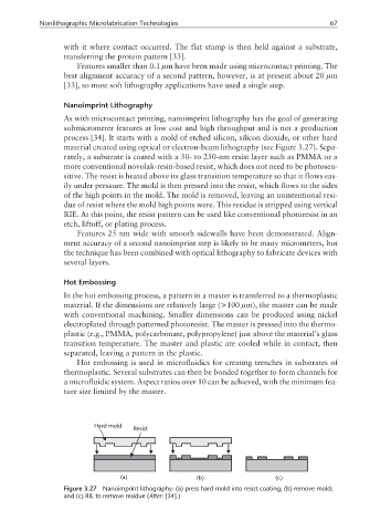
process [34]. It starts with a mold of etched silicon, silicon dioxide, or other hard
material created using optical or electron-beam lithography (see Figure 3.27). Sepa-
rately, a substrate is coated with a 50- to 250-nm resist layer such as PMMA or a
more conventional novolak-resin-based resist, which does not need to be photosen-
sitive. The resist is heated above its glass transition temperature so that it flows eas-
ily under pressure. The mold is then pressed into the resist, which flows to the sides
of the high points in the mold. The mold is removed, leaving an unintentional resi-
due of resist where the mold high points were. This residue is stripped using vertical
RIE. At this point, the resist pattern can be used like conventional photoresist in an
etch, liftoff, or plating process.
Features 25 nm wide with smooth sidewalls have been demonstrated. Align-
ment accuracy of a second nanoimprint step is likely to be many micrometers, but
the technique has been combined with optical lithography to fabricate devices with
several layers.
Hot Embossing
In the hot embossing process, a pattern in a master is transferred to a thermoplastic
material. If the dimensions are relatively large (>100 µm), the master can be made
with conventional machining. Smaller dimensions can be produced using nickel
electroplated through patterned photoresist. The master is pressed into the thermo-
plastic (e.g., PMMA, polycarbonate, polypropylene) just above the material’s glass
transition temperature. The master and plastic are cooled while in contact, then
separated, leaving a pattern in the plastic.
Hot embossing is used in microfluidics for creating trenches in substrates of
thermoplastic. Several substrates can then be bonded together to form channels for
a microfluidic system. Aspect ratios over 10 can be achieved, with the minimum fea-
ture size limited by the master.
Hard mold
Resist
(a) (b) (c)
Figure 3.27 Nanoimprint lithography: (a) press hard mold into resist coating; (b) remove mold;
and (c) RIE to remove residue (After: [34].)