
Page 93 - An Introduction to Microelectromechanical Systems Engineering
P. 93
72 Processes for Micromachining
Mask Oxide
Oxide
Resist
Silicon
1. Resist exposure 2. Etch cavity
CMOS
circuits
Silicon
Silicon Embedded
cavity
3. Silicon fusion bonding 4. Fabricate CMOS
Suspended
Anchor beam
Mask
Resist
5. Resist exposure 6. Etch (DRIE)
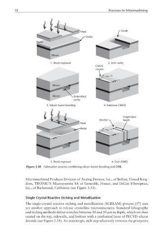
Figure 3.30 Fabrication process combining silicon fusion bonding and DRIE.
Micromachined Products Division of Analog Devices, Inc., of Belfast, United King-
dom, TRONIC’S Microsystems SA of Grenoble, France, and DiCon Fiberoptics,
Inc., of Richmond, California (see Figure 3.33).
Single Crystal Reactive Etching and Metallization
The single-crystal reactive etching and metallization (SCREAM) process [37] uses
yet another approach to release crystalline microstructures. Standard lithography
and etching methods define trenches between 10 and 50 µm in depth, which are then
coated on the top, sidewalls, and bottom with a conformal layer of PECVD silicon
dioxide (see Figure 3.34). An anisotropic etch step selectively removes the protective