Page 94 - An Introduction to Microelectromechanical Systems Engineering
P. 94

Combining the Tools—Examples of Commercial Processes                           73


                  Figure 3.31  Scanning electron microscope image of a 200-µm-deep thermal actuator fabricated
                  using silicon fusion bonding and DRIE. (Courtesy of: GE NovaSensor of Fremont, California.)
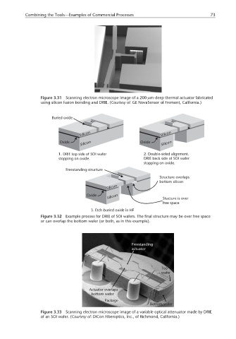

                       Buried oxide


                                   Silicon                           Silicon
                                   Silicon                            Silicon
                          Oxide                              Oxide
                          1. DRIE top side of SOI wafer       2. Double-sided alignment.
                          stopping on oxide.                  DRIE back side of SOI wafer
                                                              stopping on oxide.
                             Freestanding structure
                                                                     Structure overlaps
                                                                     bottom silicon
                                              Silicon
                                      Oxide    Silicon                Stucture is over

                                                                      free space
                                        3. Etch buried oxide in HF
                  Figure 3.32  Example process for DRIE of SOI wafers. The final structure may be over free space
                  or can overlap the bottom wafer (or both, as in this example).


                                                         Freestanding
                                                         actuator


                                                                      Top
                                                                      wafer


                                       Actuator overlaps
                                        bottom wafer
                                              Package
                                                                 Bottom wafer
                  Figure 3.33  Scanning electron microscope image of a variable optical attenuator made by DRIE
                  of an SOI wafer. (Courtesy of: DiCon Fiberoptics, Inc., of Richmond, California.)
   89   90   91   92   93   94   95   96   97   98   99