
Page 84 - An Introduction to Microelectromechanical Systems Engineering
P. 84
Nonlithographic Microfabrication Technologies 63
Photoresist First Second
plated
mask plated Substrate metal
metal
(a) (b) (c)
Figure 3.22 The EFAB process: (a) pattern photoresist and selectively electroplate first metal; (b)
blanket electroplate second metal; and (c) planarize to same thickness.
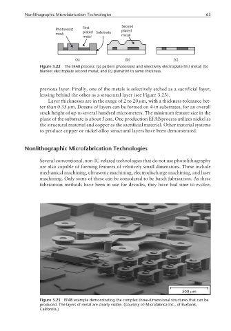
previous layer. Finally, one of the metals is selectively etched as a sacrificial layer,
leaving behind the other as a structural layer (see Figure 3.23).
Layer thicknesses are in the range of 2 to 20 µm, with a thickness tolerance bet-
ter than 0.35 µm. Dozens of layers can be formed on 4-in substrates, for an overall
stack height of up to several hundred micrometers. The minimum feature size in the
plane of the substrate is about 5 µm. One production EFABprocess utilizes nickel as
the structural material and copper as the sacrificial material. Other material systems
to produce copper or nickel-alloy structural layers have been demonstrated.
Nonlithographic Microfabrication Technologies
Several conventional, non-IC-related technologies that do not use photolithography
are also capable of forming features of relatively small dimensions. These include
mechanical machining, ultrasonic machining, electrodischarge machining, and laser
machining. Only some of these can be considered to be batch fabrication. As these
fabrication methods have been in use for decades, they have had time to evolve,
µ
500 m
Figure 3.23 EFAB example demonstrating the complex three-dimensional structures that can be
produced. The layers of metal are clearly visible. (Courtesy of: Microfabrica Inc., of Burbank,
California.)