
Page 75 - An Introduction to Microelectromechanical Systems Engineering
P. 75
54 Processes for Micromachining
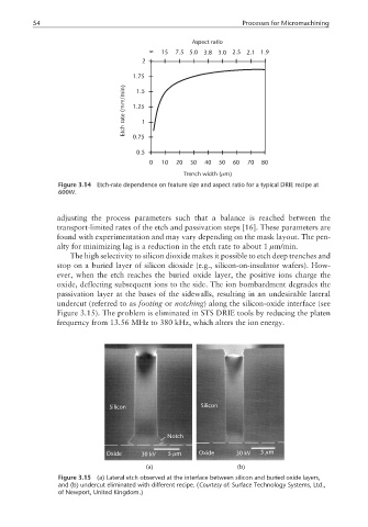
Aspect ratio
15 7.5 5.0 3.8 3.0 2.5 2.1 1.9
2
1.75
(mm/min) 1.25
1.5
rate 1
Etch
0.75
0.5
0 10 20 30 40 50 60 70 80
µ
Trench width ( m)
Figure 3.14 Etch-rate dependence on feature size and aspect ratio for a typical DRIE recipe at
600W.
adjusting the process parameters such that a balance is reached between the
transport-limited rates of the etch and passivation steps [16]. These parameters are
found with experimentation and may vary depending on the mask layout. The pen-
alty for minimizing lag is a reduction in the etch rate to about 1 µm/min.
The high selectivity to silicon dioxide makes it possible to etch deep trenches and
stop on a buried layer of silicon dioxide (e.g., silicon-on-insulator wafers). How-
ever, when the etch reaches the buried oxide layer, the positive ions charge the
oxide, deflecting subsequent ions to the side. The ion bombardment degrades the
passivation layer at the bases of the sidewalls, resulting in an undesirable lateral
undercut (referred to as footing or notching) along the silicon-oxide interface (see
Figure 3.15). The problem is eliminated in STS DRIE tools by reducing the platen
frequency from 13.56 MHz to 380 kHz, which alters the ion energy.
Silicon Silicon
Notch
µ
µ
Oxide 30 kV 5m Oxide 30 kV 5m
(a) (b)
Figure 3.15 (a) Lateral etch observed at the interface between silicon and buried oxide layers,
and (b) undercut eliminated with different recipe. (Courtesy of: Surface Technology Systems, Ltd.,
of Newport, United Kingdom.)