
Page 71 - An Introduction to Microelectromechanical Systems Engineering
P. 71
50 Processes for Micromachining
than {111} planes, thus accelerating the etch. Consequently, a convex corner in the
mask layout will be undercut during the etch; in other words, the etch front will pro-
ceed underneath the masking layer. In some instances, such as when a square island
is desired, this effect becomes detrimental and is compensated for by clever layout
schemes called corner compensation [10]. Often, however, the effect is intentionally
used to form beams suspended over cavities (see Figure 3.9).
Electrochemical Etching
The relatively large etch rates of anisotropic wet etchants (>0.5 µm/min) make it dif-
ficult to achieve uniform and controlled etch depths. Some applications, such as
bulk-micromachined pressure sensors, demand a thin (5- to 20-µm) silicon mem-
brane with dimensional thickness control and uniformity of better than 0.2 µm,
which is very difficult to achieve using timed etching. Instead, the thickness control
is obtained by using a precisely grown epitaxial layer and controlling the etch reac-
tion with an externally applied electrical potential. This method is commonly
referred as electrochemical etching (ECE) [11, 12]. An n-type epitaxial layer grown
on a p-type wafer forms a p-n junction diode that allows electrical conduction only if
the p-type side is at a voltage above the n-type; otherwise, no electrical current
passes and the diode is said to be in reverse bias. During ECE, the applied potential is
such that the p-n diode is in reverse bias, and the n-type epitaxial layer is above its
passivation potential—the potential at which a thin passivating silicon dioxide layer
forms—hence, it is not etched (see Figure 3.10). The p-type substrate is allowed to
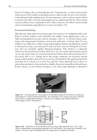
Figure 3.9 Scanning-electron micrograph of a thermally isolated RMS converter consisting of
thermopiles on a silicon dioxide membrane. The anisotropic etch undercuts the silicon dioxide
mask to form a suspended membrane. (Courtesy of: D. Jaeggi, Swiss Federal Institute of
Technology of Zurich, Switzerland.)
V
−
OH
p-Si − Electrode
OH
n-Si OH −
Figure 3.10 Illustration of electrochemical etching using n-type epitaxial silicon. The n-type
silicon is biased above its passivation potential so it is not etched. The p-type layer is etched in the
solution. The etch stops immediately after the p-type layer is completely removed.