
Page 72 - An Introduction to Microelectromechanical Systems Engineering
P. 72
Basic Process Tools 51
electrically float, so it is etched. As soon as the p-type substrate is completely
removed, the etch reaction comes to a halt at the junction, leaving a layer of n-type
silicon with precise thickness.
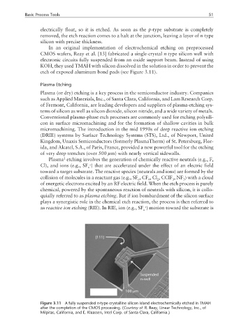
In an original implementation of electrochemical etching on preprocessed
CMOS wafers, Reay et al. [13] fabricated a single-crystal n-type silicon well with
electronic circuits fully suspended from an oxide support beam. Instead of using
KOH, they used TMAH with silicon dissolved in the solution in order to prevent the
etch of exposed aluminum bond pads (see Figure 3.11).
Plasma Etching
Plasma (or dry) etching is a key process in the semiconductor industry. Companies
such as Applied Materials, Inc., of Santa Clara, California, and Lam Research Corp.
of Fremont, California, are leading developers and suppliers of plasma-etching sys-
tems of silicon as well as silicon dioxide, silicon nitride, and a wide variety of metals.
Conventional plasma-phase etch processes are commonly used for etching polysili-
con in surface micromachining and for the formation of shallow cavities in bulk
micromachining. The introduction in the mid 1990s of deep reactive ion etching
(DRIE) systems by Surface Technology Systems (STS), Ltd., of Newport, United
Kingdom, Unaxis Semiconductors (formerly PlasmaTherm) of St. Petersburg, Flor-
ida, and Alcatel, S.A., of Paris, France, provided a new powerful tool for the etching
of very deep trenches (over 500 µm) with nearly vertical sidewalls.
2
Plasma etching involves the generation of chemically reactive neutrals (e.g., F,
+
Cl), and ions (e.g., SF ) that are accelerated under the effect of an electric field
x
toward a target substrate. The reactive species (neutrals and ions) are formed by the
collision of molecules in a reactant gas (e.g., SF ,CF ,Cl , CClF ,NF ) with a cloud
6 4 2 3 3
of energetic electrons excited by an RF electric field. When the etch process is purely
chemical, powered by the spontaneous reaction of neutrals with silicon, it is collo-
quially referred to as plasma etching. But if ion bombardment of the silicon surface
plays a synergistic role in the chemical etch reaction, the process is then referred to
as reactive ion etching (RIE). In RIE, ion (e.g., SF ) motion toward the substrate is
+
x
{111}
Suspended
n-well
100 m
µ
Figure 3.11 A fully suspended n-type crystalline silicon island electrochemically etched in TMAH
after the completion of the CMOS processing. (Courtesy of: R. Reay, Linear Technology, Inc., of
Milpitas, California, and E. Klaassen, Intel Corp. of Santa Clara, California.)