
Page 68 - Analog Circuit Design Art, Science, and Personalities
P. 68
Jim Williams
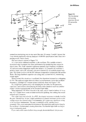
Figure 7-9.
The first attempt
at iniproving
distortion. A2 and
Q1 replace the
lamp.
seemed a.n entertaining way to stay out of the rain. Of course, I couldn't ignore that
I was already perilously near my analyzer's 0.00 18% specification limit when intcr-
preting rcsults. Not to worry.
The next circuit is shown in Figure 7-9.
A. I, a low noise wideband amplifier, is the oscillator. The variable resistor's
decreased value maintains low noise pcrfomance by minimiiing bias current in-
duced noise. Thc I0 pF capacitor suppresses parasitic high frequency oscillation,
A3 and associated components replace the lamp(s). A2 compares the osciliator's
positive peaks with a IX reference and servo-controls Q I to establish proper loop
gain. The diode in series with the DC refercncc tcmperature compensates the rectificr
diodc. The large feedback capacitor sets a long time constant for A2, minimizing
otitput ripple.
When I turned this circuit on. it oscillated. but distortion increased to a whopping
0.1 S%! The analyzer out.put showed a fierce second hannonic (twice the oscillator
frequencyj, although A2's output seemed relativcly clean (see Figure 7- 10).
So. I might have gotten away with dumping thc two tubes for94 transistors,
capacitors. arid rcsistors, but replacing the lamp with a bunch of stuff was another
matter! I looked apologetically at the forsaken light bulbs.
What happened? The Wieri network is the same; and it's hard to beliwe AI is so
bad. A3's output shows some residual rectification peaking. but nothing that would
unleash such ii monstcr.
The culprii [urns out to be Q I. In il FEI', thc channel resistance is ideally fixed by
thc gate--c.hannel bias. In fact. slight modulation of channel resistance occurs iis the
vultqy ~icross :he channel varies. Ilnfortunntely, 01 's drain sees significanr swing
at !he cscillator l'undamcntal. The gate is nominally at DC, and thc sourcc
grounded. This ciiuses unwanted modulation of the amplitude stabilization loop by
the oscilititor's I'undamental, creating distortion. The humble light bulb was bcgin-
ning ti) iook pretty good.
If yc?u stare at this state of affairs Ions cnough, the needed Band-Aid prcscnis
49