Page 197 - Analog and Digital Filter Design
P. 197
1 94 Analog and Digital Filter Design


                                   6J
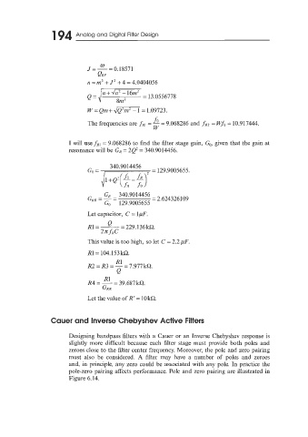
                              J  =  ~   = 0.18571
                                  QBP
                              n = m2 + J'  + 4 = 4.0404056
                              Q=d       8nz2     = 13.0556778
                                   n -t 2/12'  - 16m2

                              H7 = Qnz +  4-    = 1.09723.

                              The frequencies are fR1=  f. = 9.068286 and fRZ  = W&  = 10.917444.
                                                    w

                        I will use fRI  = 9.068286 to find the filter stage gain, Go, given that the gain at
                        resonance will be GR  = 2@ = 340.9014456.

                                      340.9014456
                                                    = 129.9005655.
                                    l+Q-
                                          fR  fo


                              Let capacitor,  C = IpF.
                                     A


                              This value is too high, so let C = 2.2 pF.
                              R1= 104.153kQ.
                                        R1
                              R2 = R3 = - = 7.977kQ.
                                        Q
                                    R1
                              R4 = - 39.687kQ.
                                       =
                                   GRR
                              Let the value of R' = 10 kQ.


                  Cauer and Inverse Chebyshev Active Filters

                        Designing bandpass filters with a Cauer or an Inverse Chebyshev response is
                        slightly more difficult because  each filter stage must  provide both  poles and
                        zeroes close to the filter center frequency. Moreover, the pole and zero pairing
                        must  also  be  considered.  A  filter may  have  a  number  of  poles  and  zeroes
                        and, in principle, any zero could be associated with any pole. In practice the
                        pole-zero pairing  affects performance. Pole and zero pairing  are illustrated in
                        Figure 6.14.

