
Page 193 - Analog and Digital Filter Design
P. 193
1 90 Analog and Digital Filter Design
R3
Using the equations, Rl = - = 55.139 kQ and R2 = R3 = 1.048w2.
2. GRR 4Q2 -2G,,
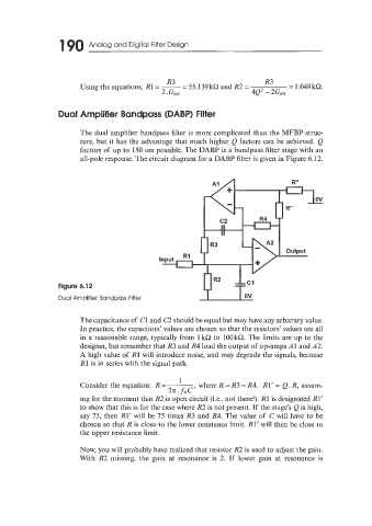
Dual Amplifier Bandpass (DABP) Filter
The dual amplifier bandpass filter is more complicated than the MFBP struc-
ture, but it has the advantage that much higher Q factors can be achieved. Q
factors of up to 150 are possible. The DABP is a bandpass filter stage with an
all-pole response. The circuit diagram for a DABP filter is given in Figure 6.12.
Figure 6.12
Dual Amplifier Bandpass Filter
The capacitance of C1 and C2 should be equal but may have any arbitrary value.
In practice, the capacitors’ values are chosen so that the resistors’ values are all
in a reasonable range, typically from 1 kC2 to 100kQ. The limits are up to the
designer, but remember that R3 and R4 load the output of op-amps A1 and A2.
A high value of R1 will introduce noise, and may degrade the signals, because
R1 is in series with the signal path.
1
Consider the equation: R = ~ where R = R3 = R4. R1‘ = Q. R, assum-
2n. fRc’
ing for the moment that R2 is open circuit (i.e., not there!). R1 is designated R1’
to show that this is for the case where R2 is not present. If the stage’s Q is high,
say 75, then R1‘ will be 75 times R3 and R4. The value of C will have to be
chosen so that R is close to the lower resistance limit. R1’ will then be close to
the upper resistance limit.
Now, you will probably have realized that resistor R2 is used to adjust the gain.
With R2 missing, the gain at resonance is 2. If lower gain at resonance is