
Page 190 - Analog and Digital Filter Design
P. 190
Bandpass Filters 187
If the desired midband gain is greater than unity, given by factor k. then GRR
~GR
. To achieve this scaling, the poten-
must also be scaled by factor k: GRR = -
Gu
tial divider is modified to allow a greater proportion of the input signal into the
filter stage.
If a number of stages are used, the overall midband gain will be the product of
all the separate stage gains: G, = G1 *G2*G3 *, and so on. If each stage has a
gain that is not unity at the filter center frequency, an inverting amplifier fol-
lowing the filter stages with a gain of 1/G, could be used to restore the overall
filter gain to unity.
Multiple Feedback Bandpass Filter
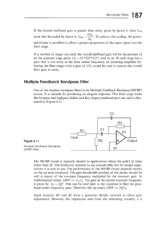
One of the simplest bandpass filters is the Multiple Feedback Bandpass (MFBP)
circuit. It is suitable for producing an all-pole response. This filter stage looks
Like lowpass and highpass Sallen and Key stages combined into one and is illus-
trated in Figure 6.11.
c2
Figure 6.1 1
Multiple Feedback Bandpass
JviFBP) Filter
The MFBP circuit is typically limited to applications where the pole’s (2 value
is less than 20. This limitation restricts its use considerably, but for simple appli-
cations it is easy to use. The performance of the MFBP circuit depends mainly
on the op-amp employed. The gain-bandwidth product of the device should be
well in excess of the resonant frequency multiplied by the resonant gain. In
mathematical terms: GBW>> GR fR. The gain at the circuit resonant frequency
is given by: GR = 2Q’. This can be used later in the equation to find the pass-
band center frequency gain. Therefore the op-amp’s GBW>> 2Q”fR.
Input resistors R1 and R2 form a potential divider network to allow gain
adjustment. However, the impedance seen from the remaining circuitry is a