
Page 185 - Analog and Digital Filter Design
P. 185
1 82 Analog and Digital Filter Design
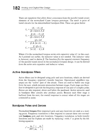
There are equations that allow direct conversion from the parallel tuned circuit
elements of the normalized Cauer lowpass prototype. The result is pairs of
tuned circuits for the denormalized bandpass filter. These are given below:
Where Xis the normalized lowpass series arm capacitor value (Cz in this case).
As I pointed out earlier, the inductor value is not needed. The inductor value
is, however, used to derive p. The function p is the squared resonant frequency
of the parallel tuned circuit in the normalized lowpass design. It can be derived
from the series arm capacitor and inductor values.
Active Bandpass Filters
Active filters can be designed using pole and zero locations, which are derived
from the frequency response’s transfer function. Operational amplifiers (op-
amps) are the “active” part of the circuit. These are used to buffer one stage
from the next, which prevents interaction between stages. Each stage can there-
fore be designed to provide the frequency response of one pair of complex poles.
Zeroes are also required, above and below the passband. Active networks used
in bandpass filter circuits also produce zeroes. Because each filter stage is
buffered from the next, the overall response is correct when all the stages are
connected in series.
Bandpass Poles and Zeroes
Normalized lowpass filter response’s pole and zero locations are used as a start-
ing point. Frequency translation is then required to convert these into normal-
ized bandpass pole and zero locations. Frequency translation in both transfer
functions and the S-plane are made by replacing s with s” as given by the fol-
lowing equation: