
Page 181 - Analog and Digital Filter Design
P. 181
1 78 Analog and Digital Filter Design
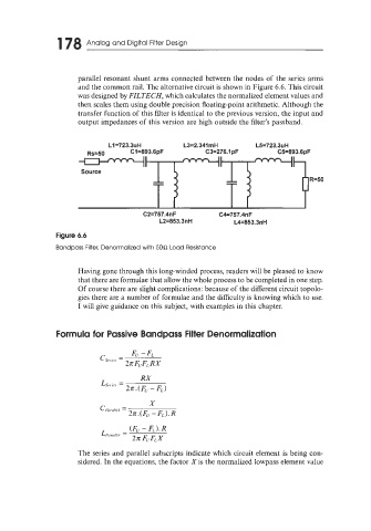
parallel resonant shunt arms connected between the nodes of the series arms
and the common rail. The alternative circuit is shown in Figure 6.6. This circuit
was designed by FILTECH, which calculates the normalized element values and
then scales them using double precision floating-point arithmetic. Although the
transfer function of this filter is identical to the previous version, the input and
output impedances of this version are high outside the filter's passband.
L1=723.3uH L3=2.341mH L5=723.3uH
C1=893.6pF C3=276.1 pF C5=893.6pF
Source
R=50
C2=757.4nF C4=757.4nF
L2=853.3nH L4=853.3nH
Figure 6.6
Bandpass Filter, Denormalized with 50R Load Resistance
Having gone through this long-winded process, readers will be pleased to know
that there are formulae that allow the whole process to be completed in one step.
Of course there are slight complications: because of the different circuit topolo-
gies there are a number of formulae and the difficulty is knowing which to use.
I will give guidance on this subject, with examples in this chapter.
Formula for Passive Bandpass Filter Denormalization
(Fu - FL).R
LPm,lkl =
22~ FUFLX
The series and parallel subscripts indicate which circuit element is being con-
sidered. In the equations, the factor Xis the normalized lowpass element value