
Page 180 - Analog and Digital Filter Design
P. 180
Bandpass Filters 1 77
The capacitor and inductor values given are for a normalized 1 R load. Denor-
malization of the bandpass model for higher load impedance requires compo-
nent values to be scaled to have higher impedance. This is done in exactly thc
same way that lowpass or highpass filters are scaled. Inductor values increase
in proportion to the load impedance and capacitor values reduce in inverse pro-
portion to the load. Capacitor values reduce because their impedance is inversely
proportional to their capacitance values. As the load impedance increases, all
the reactances in the circuit must increase in order to have the same response as
the model.
The filter you have been designing is intended to provide a filter for a simple
radio receiver, to pick up a carrier at 198 kHz. This requires a 5051 source and
load impedance, to match the radio frequency components at its input and
output (50R is the standard impedance for RFcircuits; 75R is standard for tel-
evision picture transmission). Impedance scaling is achieved by multiplying the
inductor values by 50 and dividing the capacitor by 50. Finally, the filter circuit
given in Figure 6.5 is obtained.
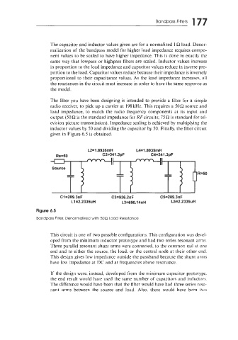
C1=289.3nF C3=936.2nF C5=289.3nF
L1=2.2335u H L3=690.14nH L5=2.2335uH
Figure 6.5
Bandpass Filter, Denormalized with 50R Load Resistance
This circuit is one of two possible configurations. This configuration was devel-
oped from the minimum inductor prototype and had two series resonant arms.
Three parallel resonant shunt arms were connected. to the common rail at one
end and to either the source, the load. or the central node at their other end.
This design gives low impedance outside the passband because the shunt arms
have low impedance at DC and at frequencies above resonance.
If the design were. instead. developed from the minimum capacitor prototype.
the end result would have used the same number of capacitors and inductors.
The difference would have been that the filter would have had three series reso-
nant arms between the source and load. Also. there would have been two