
Page 183 - Analog and Digital Filter Design
P. 183
1 80 Analog and Digital Filter Design
4 -FL
CS,,,,'.\ = 6.8 x 10'/7.609233 x 10" = 893.6pF
=
27tF"FLRX
L- - RX - 20 9142,72566 = 723.2,uH
A shunt arm must be calculated next, using X= 1.618, followed by another series
arm, using X= 2.0. Because of symmetry, the final two arms will have the same
component values as previously calculated for the first two arms. The last arm
will have the same component values as the first arm. The one-before-last arm
will have the same component values as the second arm.
Passive Cauer and Inverse Chebyshev Bandpass Filters
So far, procedures for designing all-pole bandpass filters have been explained.
However, Cauer and Inverse Chebyshev responses have zeroes in the stopband,
so their circuit topology must be more complex. I have shown in earlier
chapters that designing for lowpass or highpass Cauer filters is straightforward.
This is because the zeroes are scaled outward from the S-plane origin in the
lowpass case. Zeroes are inverted and then scaled to be less than the cutoff fre-
quency in the highpass case. Zeroes in the resultant passive filter are produced
by parallel resonant circuits in the series arm, or series resonant circuits in the
shunt arm.
When it comes to designing Cauer bandpass filters, two zeroes are required for
each zero in the lowpass prototype, one above and one below the passband fre-
quency range. This means that two resonant circuits are required in the band-
pass filter for each one in the lowpass prototype. The procedure for finding these
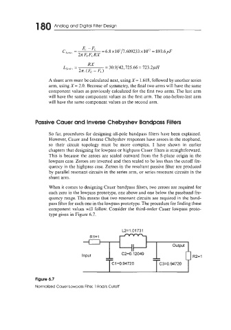
component values will follow. Consider the third-order Cauer lowpass proto-
type given in Figure 6.7.
II output
I
-- -- R2= 1
--
--
Input C2=0.12049
C1=0.94720 C3=0.94720
Figure 6.7
Normalized Cauer Lowpass Filter, 1 Rad/s Cutoff