Page 195 - Analog and Digital Filter Design
P. 195
1 92 Analog and Digital Filter Design


                                                   fo
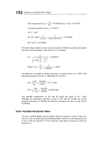
                              The frequencies are fR,  = - 9.57306 and fR2 = Wfo = 10.34178.
                                                      =
                                                   w
                              Consider the pole with  fR2  = 10.34178.
                              Let c = 1pF


                              Rl‘=Q.R= 82.928kQ.

                       Note that these values are less than the nominal 100 kQ maximum and greater
                       than the 1 kC2  minimum, so the value of  C is suitable.


                                          GR       2
                              Hence, GRR  = -           = 1 .OS32
                                             =
                                          Go   1.8463811
                       An attenuator is needed to reduce the gain at resonance from 2 to 1.0832. The
                       following equations use R1’ to determine R1 and R2:


                       The  parallel  combination  of  R1  and  R2  equal  the  value  of  Rl’.  Thus,
                       although  the  individual resistance values of  R1  and  R2  exceed  the  recom-
                       mended maximum of  100 kQ, the effective resistance into the op-amp will be
                        82.928  kQ.


                 State Variable Bandpass Filters

                       The state variable design can be used for all-pole responses. It has a lower sen-
                       sitivity to the op-amp’s gain-bandwidth product limitation, and stage Q factors
                       of  up to 200 are possible. It does, however, need three op-amps, as shown in
                       Figure 6.13.

