
Page 240 - Analog and Digital Filter Design
P. 240
Impedance Matching Networks
Bandpass Matching into a Single Reactance Load
One of the most conmon impedance matching problems is to match a resistive
source into a load comprising a resistance and a parallel capacitance. If the load
capacitor can be somehow absorbed into the matching network design, the
problem then reduces to simple resistive matching. A suitable matching network
in this case will have a shunt capacitance across the load terminals. This could
be a lowpass PI network, or a type-A lowpass L network.
There is a simple condition for being able to match a resistive source to a load
comprising a resistance and a parallel capacitance. It is that the shunt capaci-
tance of the load must be smaller than the shunt capacitance of the matcbing
network. The circuit is designed to match the source and load resistance. This
design produces a certain value of load shunt capacitance. If the load is applied.
the capacitance of the load and the capacitance of the matching network add
together, giving too great a value. This can be corrected by subtracting the load
capacitance from the shunt capacitance of the matching circuit. Thus the load
capacitance forms part of the resistive impedance matching circuit.
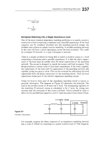
Using [he load to form part of the impedance matching circuit is known as
parasitic absorption. The diagram in Figure 8.9 illustrates the principle. The
load is the parallel circuit of R load and C load. The terminating capacitor in
the matching PI network shown is calculated to be C term, by taking into
account only the resistance of the source and load. This is reduced in value to
allow for the parallel load capacitor, and its value becomes Cterrn minus Cload.
C = Cterm - Cload
\ I
Figure 8.9
Parasitic AbsorDtion
For example, suppose the shunt capacitor of an impedance matching network
has a value of lOOpF for matching to a purely resistive load of 75Q. Suppose.