
Page 237 - Analog and Digital Filter Design
P. 237
234 Analog and Digital Filter Design
t T“
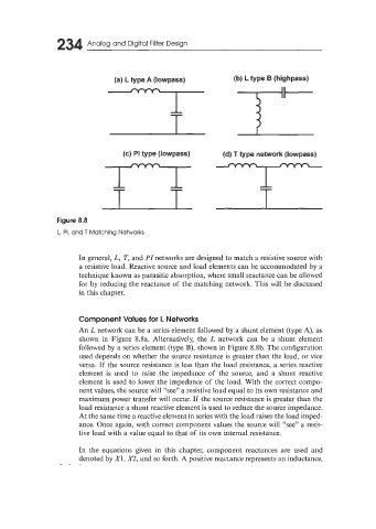
(a) L type A (lowpass) (b) L type B (highpass)
I
(c) PI type (lowpass) (d) T type network (lowpass)
fl
-I-
T
Figure 8.8
L, PI, and T Matching Networks
In general, L, T, and PI networks are designed to match a resistive source with
a resistive load. Reactive source and load elements can be accommodated by a
technique known as parasitic absorption, where small reactance can be allowed
for by reducing the reactance of the matching network. This will be discussed
in this chapter.
Component Values for L Networks
An L network can be a series element followed by a shunt element (type A), as
shown in Figure 8.8a. Alternatively, the L network can be a shunt element
followed by a series element (type B), shown in Figure 8.8b. The configuration
used depends on whether the source resistance is greater than the load, or vice
versa. If the source resistance is less than the load resistance, a series reactive
element is used to raise the impedance of the source, and a shunt reactive
element is used to lower the impedance of the load. With the correct compo-
nent values, the source will “see” a resistive load equal to its own resistance and
maximum power transfer will occur. If the source resistance is greater than the
load resistance a shunt reactive element is used to reduce the source impedance.
At the same time a reactive element in series with the load raises the load imped-
ance. Once again, with correct component values the source will “see” a resis-
tive load with a value equal to that of its own internal resistance.
In the equations given in this chapter, component reactances are used and
denoted by X1, X2, and so forth. A positive reactance represents an inductance,