
Page 233 - Analog and Digital Filter Design
P. 233
230 Analog and Digital Filter Design
The source impedance is not taken into account in the design of diplexers. This
is because the diplexer has two filters, with the same cutoff frequency, connected
together. When the signal frequency increases beyond the passband edge of one
filter, which then has high input impedance, the other filter provides a termina-
tion. The two filter sections together provide constant input impedance at all
frequencies. This means that the source voltage does not rise outside the pass-
band. From the point of view of each filter section, this is equivalent to the
source voltage having no impedance; that is, it remains constant even when the
input impedance of the filter is rising. Therefore a filter designed for a zero
source impedance (constant input voltage) is used.
The normalized design can be used to produce highpass/lowpass diplexer filter
section designs using the information given in the earlier chapters. First, select
a set of normalized component values given for zero source impedance from the
tables given in Chapter 3. The normalized design must be scaled for frequency
and impedance, as described in Chapters 4 to 7, to produce a lowpass section.
One filter section must then be transformed into a highpass response. As a check,
if the values of the first series components of both sections are multiplied
together, the product will be equal to the reciprocal of w,, the cutoff frequency.
Similarly, the products of the second and third pair of component values are
also equal to the reciprocal of w,. Bandpass-bandstop diplexers can be designed
in a similar way. The normalized lowpass filter must be frequency and imped-
ance scaled. Transformation into bandpass and bandstop sections is then
required.
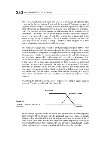
Analyzing the combined circuit can be achieved by using a circuit analysis
program. The plot should look like Figure 8.6.
. . . . . . . . . . . . .
Amplitude
Figure 8.6
Diplexer Combined Frequency
Response Frequency
More complex diplexers can be produced, with perhaps four or more frequency
band outputs. These diplexers can be produced using two stages of simple
diplexers; thus a band could be split into upper and lower frequencies. Both of
these bands could then be split into upper and lower frequencies. This would
result in four frequency band outputs. It would be wise to simulate such circuits
before building them, because multichannel diplexers can be expensive.