
Page 64 - Analytical Electrochemistry 2d Ed - Jospeh Wang
P. 64
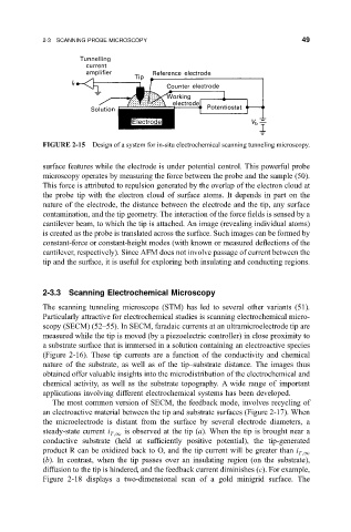
2-3  SCANNING PROBE MICROSCOPY                                   49


            FIGURE 2-15 Design of a system for in-situ electrochemical scanning tunneling microscopy.


            surface features while the electrode is under potential control. This powerful probe
            microscopy operates by measuring the force between the probe and the sample (50).
            This force is attributed to repulsion generated by the overlap of the electron cloud at
            the probe tip with the electron cloud of surface atoms. It depends in part on the
            nature of the electrode, the distance between the electrode and the tip, any surface
            contamination, and the tip geometry. The interaction of the force ®elds is sensed by a
            cantilever beam, to which the tip is attached. An image (revealing individual atoms)
            is created as the probe is translated across the surface. Such images can be formed by
            constant-force or constant-height modes (with known or measured de¯ections of the
            cantilever, respectively). Since AFM does not involve passage of current between the
            tip and the surface, it is useful for exploring both insulating and conducting regions.


            2-3.3  Scanning Electrochemical Microscopy

            The scanning tunneling microscope (STM) has led to several other variants (51).
            Particularly attractive for electrochemical studies is scanning electrochemical micro-
            scopy (SECM) (52±55). In SECM, faradaic currents at an ultramicroelectrode tip are
            measured while the tip is moved (by a piezoelectric controller) in close proximity to
            a substrate surface that is immersed in a solution containing an electroactive species
            (Figure 2-16). These tip currents are a function of the conductivity and chemical
            nature of the substrate, as well as of the tip±substrate distance. The images thus
            obtained offer valuable insights into the microdistribution of the electrochemical and
            chemical activity, as well as the substrate topography. A wide range of important
            applications involving different electrochemical systems has been developed.
              The most common version of SECM, the feedback mode, involves recycling of
            an electroactive material between the tip and substrate surfaces (Figure 2-17). When
            the microelectrode is distant from the surface by several electrode diameters, a
            steady-state current i  is observed at the tip (a). When the tip is brought near a
                             T;1
            conductive substrate (held at suf®ciently positive potential), the tip-generated
            product R can be oxidized back to O, and the tip current will be greater than i
                                                                            T;1
            (b). In contrast, when the tip passes over an insulating region (on the substrate),
            diffusion to the tip is hindered, and the feedback current diminishes (c). For example,
            Figure 2-18 displays a two-dimensional scan of a gold minigrid surface. The