
Page 230 - Build Your Own Quadcopter_ Power Up Your Designs with the Parallax Elev-8
P. 230
Chapter 8: GPS and a Real- T ime Situational Displa y 209
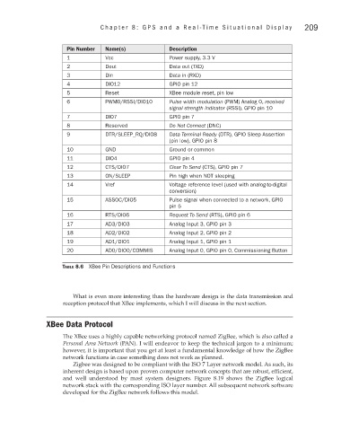
Pin Number Name(s) Description
1 Vcc Power supply, 3.3 V
2 Dout Data out (TXD)
3 Din Data in (RXD)
4 DIO12 GPIO pin 12
5 Reset XBee module reset, pin low
6 PWM0/RSSI/DIO10 Pulse width modulation (PWM) Analog 0, received
signal strength indicator (RSSI), GPIO pin 10
7 DIO7 GPIO pin 7
8 Reserved Do Not Connect (DNC)
9 DTR/SLEEP_RQ/DIO8 Data Terminal Ready (DTR), GPIO Sleep Assertion
(pin low), GPIO pin 8
10 GND Ground or common
11 DIO4 GPIO pin 4
12 CTS/DIO7 Clear To Send (CTS), GPIO pin 7
13 ON/SLEEP Pin high when NOT sleeping
14 Vref Voltage reference level (used with analog-to-digital
conversion)
15 ASSOC/DIO5 Pulse signal when connected to a network, GPIO
pin 5
16 RTS/DIO6 Request To Send (RTS), GPIO pin 6
17 AD3/DIO3 Analog Input 3, GPIO pin 3
18 AD2/DIO2 Analog Input 2, GPIO pin 2
19 AD1/DIO1 Analog Input 1, GPIO pin 1
20 AD0/DIO0/COMMIS Analog Input 0, GPIO pin 0, Commissioning Button
Table 8.6 XBee Pin Descriptions and Functions
What is even more interesting than the hardware design is the data transmission and
reception protocol that XBee implements, which I will discuss in the next section.
XBee Data Protocol
The XBee uses a highly capable networking protocol named ZigBee, which is also called a
Personal Area Network (PAN). I will endeavor to keep the technical jargon to a minimum;
however, it is important that you get at least a fundamental knowledge of how the ZigBee
network functions in case something does not work as planned.
Zigbee was designed to be compliant with the ISO 7 Layer network model. As such, its
inherent design is based upon proven computer network concepts that are robust, efficient,
and well understood by most system designers. Figure 8.19 shows the ZigBee logical
network stack with the corresponding ISO layer number. All subsequent network software
developed for the ZigBee network follows this model.