
Page 122 - Build Your Own Transistor Radios a Hobbyists Guide to High-Performance and Low-Powered Radio Circuits
P. 122
Converter Det
RF Antenna Filter IF Filter 1 IF Amplifier IF Filter 2
~ VC1_ Osc ~ ~ -7 ~ L,evel Shifter ~
/ / / /
VC1 RF/L 1 T2 IF Q2 T3 IF
T1 OsclQ1 0304 R5
/ I"
fVCI RF +VCI~C
/ 140pf / 60pf AVCVoltage
---- Low Pass Filter 1/
R4C4 I"
= = Audio Coupling Capacitor C7
Audio Amplifier
~
/
Q3Q4
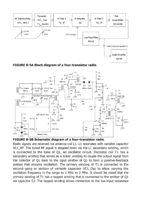
FIGURE 8-5A Block diag1ram of a four-transistor radio.
+3
R5
20K
04
lN9141N914
n • L1 Secondary R4
11 _un '-__ -J 10K
I
ca
1 ut
+ 3 421Fl00 Pin Out
RI ToT2 6 3
C12
220 ut
2 ToC2
01
R6
1N914 To Ql 4 VC10sc
20K
02
1N914 Bottom View
FIGURE 8-58 Schematic diagram of a four-transistor radio.
Radio signals are received via antenna coil Ll. L1 resonates with variable capacitor
VC1_RF. The tuned RF signal is stepped down via the L1 secondary winding, which
is connected to the base of Ql, an oscillator circuit. Oscillator coil T1 has a
secondary winding that serves as a tickler winding to couple the output signal from
the collector of Q1 back to the input emitter of Ql to form a positive-feedback
system that ensures oscillation. The primary winding of T1 is connected to the
second gang or section of variable capacitor VC1_0sc to allow varying the
oscillation frequency in the range to 1 MHz to 2 MHz. It should be noted that the
primary winding of T1 has a tapped winding that is connected to the emitter of Ql
via capacitor C2. The tapped winding allows connection to the low-input resistance