Page 142 - Build Your Own Transistor Radios a Hobbyists Guide to High-Performance and Low-Powered Radio Circuits
P. 142

+ 1.5
                                                                                 ,01  uf

            VC1RF   VCl  RF Pad
                                                                                                         Ra
            270 pr    20 pr                                                                        C13
                                                                                                          lOOK
                                          C7  + 1 ,5     Q4                                       .0022 uf
                                                  T2
                            •  L l'  Primary           MPSH10  (I')
                                                 4
                              330 Uh
                                           r---..---(2IiC   2
                                                                                              C14       1.1  M
                                                                                              1 ut
                                                                                                    + 1.5
                   R13

                   lOOK
             VC l  Osc   VCl  Osc Pad   T1
                                                                + 1,5
                         20 pr
                                                         33~         R4              R10
                    C16
                   330 pt                                    R3      56K             lOOK
                                                                              e10
                    -Pri                                     56K               ~

                                                                     01      .01 ut
                           rh  Cl                                    lN9l4
                                                                              Note #  2:  Use Low SI de Tap for T2. T3 & T 4
                               ,01  uf                               02
                                                                     lN914
             Note #  1:  For 421Fl 01 ,Tl
             Vel_Osc Pad  0  Low Side
             Tap ofT 1 ,
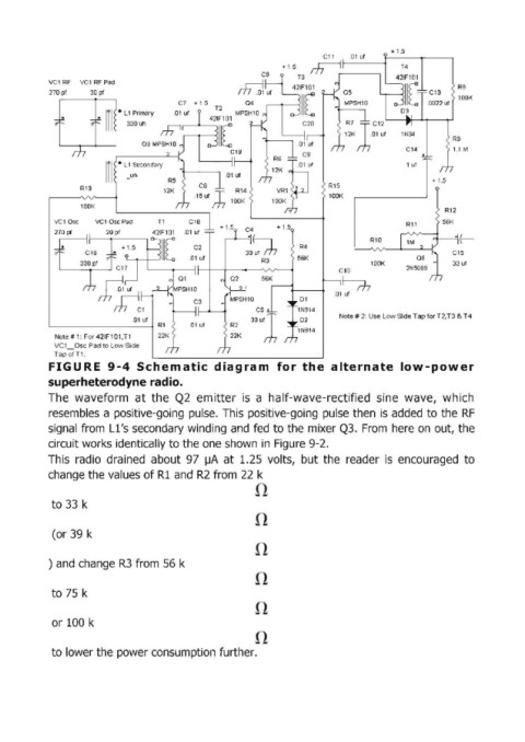
            FIGURE  9-4  Schematic  diagram  for  the  alternate  low-power
            superheterodyne radio.
            The  waveform  at  the  Q2  emitter  is  a  half-wave-rectified  sine  wave,  which
            resembles  a positive-going  pulse.  This  positive-going  pulse then  is  added  to  the  RF
            signal  from  Ll's secondary winding  and  fed  to the mixer Q3.  From  here on  out,  the
            circuit works identically to the one shown  in  Figure 9-2.

            This  radio  drained  about  97  ~A at  1.25  volts,  but  the  reader  is  encouraged  to
            change the values of RI  and  R2 from  22 k


             to  33  k


             (or 39  k


            ) and  change R3  from  56 k


             to  75  k


             or 100 k


             to lower the power consumption  further.
   137   138   139   140   141   142   143   144   145   146   147