
Page 78 - Building A Succesful Board-Test Strategy
P. 78
64 BUILDING A SUCCESSFUL BOARD-TEST STRATEGY
Receiver
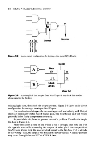
Figure 2-8 An in-circuit configuration for testing a two-input NAND gate.
Set(S)
Figure 2-9 A noise glitch that escapes from NAND-gate B may look like another
clock signal to the flip-flop.
existing logic state, then reads the output pattern. Figure 2-8 shows an in-circuit
configuration for testing a two-input NAND gate.
For combinational designs, the in-circuit approach works fairly well. Output
states are reasonably stable. Good boards pass, bad boards fail, and test results
generally indict faulty components accurately.
Sequential circuits, however, present more of a problem. Consider the simple
flip-flop in Figure 2-9.
Most tests assert a state on the D line, clock it through, then hold the D in
the opposite state while measuring the outputs. A noise glitch that escapes from
NAND-gate B may look like another clock signal to the flip-flop. If D is already
in the "wrong" state, the outputs will flip and the device will fail. A similar problem
may occur from glitches on SET or CLEAR lines.