
Page 134 - Carbon Nanotubes
P. 134
124 J.-P. ISSI et al.
nanotube structures like microbundles, or even better,
single nanotubes. A rather sophisticated technique,
namely submicronic lithographic patterning of gold
films with a scanning tunneling microscope[ 181, was
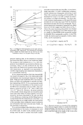
developed by Langer et al. [ 191 to attach two electri-
cal contacts to a single microbundle. This direct elec-
trical resistance measurement on this quasi-1D system
excludes the errors that may result from the situations
described in (2) and (4) in the last paragraph. The re-
ported temperature dependence measured from 300 K
down to 0.3 K by Langer et al. [19] is shown in Fig. 5.
Above 2 K, some interesting information was obtained
by fitting the experimental zero-field resistance data
to a simple two-band (STB) model successfully applied
by Klein[20-22] to semimetallic graphite. In this STB-
model, the electron and hole densities, n andp, respec-
tively, can be expressed by:
p = C,k,Tln[l + exp[(A - EF)/kBTII (2)
Fig. 4. (a) Magnetic field dependence of the high- and low-
temperature MR, respectively. The solid lines are calculated
using a simple two-band model for (a) and the 2D weak 500 I , , , , . 1 1
localization theory for (b) (after Song et a/.[16]). I
perature implying that, as the temperature increases
the Fermi level shifts closer to the conduction band.
The increase in total conductivity, a, + up, with tem-
perature was attributed to an increase in electron con- 400
centration. Song et al. [16] attributed the fact that
above 60 K the conductivity increases almost linearly 1
with temperature, as opposed to an exponential or
variable range hopping-type temperature dependence, - I11 I1
to a semimetallic behavior. 8
At low temperature and low field, the observed MR Y
was found to be negative, Fig. 4 (b), while positive MR 2
contributions were increasingly important for higher
fields. While 1D weak localization (WL) was found by
Song et al. [lq to be inadequate to describe the data,
they claimed that 2D WL fit the experimental results
for the temperature dependence of the resistivity and
the MR at low temperature and low fields. They esti- '8
mated a resistivity of 0.65 x lop4 Qm at 300 K and 0%
w
1.6 x Om at 5 K. However, the actual resistivity I
of the metallic tubules along their axis should be much
lower than these values for many reasons: (1) as pre-
dicted by the theory described in [7], only one third
of the tubules are conducting; (2) the filling factor of
a large bundle like the measured one is less than 1; (3)
when the tubes are not single-walled, the cross-section
of the nanotubes where conduction occurs is unknown
and affected by their inner structure and, finally, (4)
the nanotube is anisotropic.
To avoid the problems described above relative to
the interpretation of the results, it is necessary to work
at a lower scale. In other words, modern nanotech-
nology must be used to contact electrically smaller