
Page 133 - Carbon Nanotubes
P. 133
Electronic properties of carbon nanotubes 123
ing attributed to [I/(&, - E)’”] -type singularities in diameter and a few pm length. Second, this sample
the 1D density of states seen in the density of states with its contacts must be characterized to determine
versus energy diagrams calculated in[8]. Several I-V its exact diameter and helicity. To take up this chal-
curves were collected along the length of each tube. lenge it is necessary to resort to nanotechnologies.
Reproducible spectra were obtained on 9 tubes with Before reviewing the results of different measure-
different diameters. ments, we need to first briefly describe the nature of
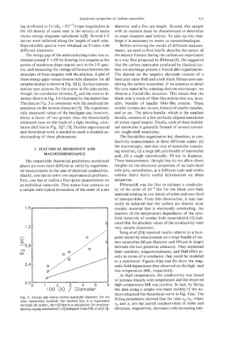
The energy gap of the semiconducting tubes was es- the deposit formed during the carbon-arc experiment
timated around V = 0 V by drawing two tangents at the in a way first proposed by EbbesentS]. He suggested
points of maximum slope nearest zero in the I-V spec- that the carbon nanotubes produced by classical car-
tra, and measuring the voltage difference between the bon arc-discharge present a fractal-like organization.
intercepts of these tangents with the abscissa. A plot of The deposit on the negative electrode consists of a
these energy gaps versus inverse tube diameter for all hard gray outer shell and a soft black fibrous core con-
samples studied is shown in Fig. 3[11]. Surface contam- taining the carbon nanotubes. If we examine in detail
ination may account for the scatter in the data points, this core material by scanning electron microscopy, we
though the correlation between Eg and the inverse di- observe a fractal-like structure. This means that the
ameter shown in Fig. 3 is illustrated by the dashed line. black core is made of fiber-like entities that are, in re-
The data in Fig. 3 is consistent with the predicted de- ality, bundles of smaller fiber-like systems. These
pendence on the inverse diameter[ 131. The experimen- smaller systems are, in turn, formed of smaller bundles,
tally measured values of the bandgaps are, however, and so on. The micro-bundle, which is the smallest
about a factor of two greater than the theoretically bundle, consists of a few perfectly aligned nanotubes
estimated ones on the basis of a tight binding calcu- of almost equal lengths. Finally, each of these individ-
lation (full line in Fig. 3)[7,13]. Further experimental ual nanotubes is generally formed of several concen-
and theoretical work is needed to reach a detailed un- tric single-shell nanotubes.
derstanding of these phenomena. The fractal-like organization led, therefore, to con-
ductivity measurements at three different scales: (1)
the macroscopic, mm-size core of nanotube contain-
3. ELECTRICAL RESISTIVITY AND ing material, (2) a large (60 pm) bundle of nanotubes
MAGNETORESISTANCE
and, (3) a single microbundle, 50 nm in diameter.
The remarkable theoretical predictions mentioned These measurements, though they do not allow direct
above are even more difficult to verify by experimen- insights on the electronic properties of an individuai
tal measurements in the case of electrical conductivity. tube give, nevertheless, at a different scale and within
Ideally, one has to solve two experimental problems. certain limits fairly useful information on these
First, one has to realize a four-point measurement on properties.
an individual nanotube. That means four contacts on Ebbesen[4] was the first to estimate a conductiv-
a sample with typical dimensions of the order of a nm ity of the order of Qm for the black core bulk
material existing in two thirds of tubes and one third
of nanoparticles. From this observation, it may nat-
urally be inferred that the carbon arc deposit must
1.6 contain material that is electricaliy conducting. An
analysis of the temperature dependence of the zero-
field resistivity of similar bulk materials[ 14,151 indi-
cated that the absolute values of the conductivity were
1.2 very sample dependent.
Song et al. [16] reported results relative to a four-
n point resistivity measurement on a large bundle of car-
3 bon nanotubes (60 pm diameter and 350 pm in length
-0.8 between the two potential contacts). They explained
their resistivity, magnetoresistance, and Hall effect re-
sults in terms of a conductor that could be modeled
as a semimetal. Figures 4 (a) and (b) show the mag-
netic field dependence they observed on the high- and
low-temperature MR, respectively.
At high temperature, the conductivity was found
to increase linearly with temperature and the observed
high-temperature MR was positive. In fact, by fitting
the data using a simple two-band model[l7] the au-
thors obtained the theoretical curve in Fig. 4 (a). The
Fig. 3. Energy gap versus inverse nanotube diameter, for the fitting parameters showed that the ratio u,/a,, where
nine nanotubes studied; the dashed line is a regression
through the points, the full line is a calculation for semicon- up and a, are the partial conductivities of holes and
ducting zigzag nanotubes[7,13] (adapted from Olk et aL[ll]). electrons, respectively, decreases with increasing tem-