
Page 78 - Complete Wireless Design
P. 78
Modulation
Modulation 77
phase distortions of the signal through phase cancellation, decreasing the
received signal strength—which decreases SNR, and thus increases the BER.
Therefore, digitally modulated radio systems must be designed for low lev-
els of phase noise, group delay variations, IMD, amplitude ripple and shape,
frequency variations, and multipath and high levels of SNR so as not to
adversely influence the BER of phase/amplitude-modulated digital signals.
Another very important issue in digital modulation that has, as yet, only
been touched on is the effect that the filtering within the transmitter’s modu-
lator has on digital signals. This filtering, as stated above, is employed to lim-
it transmitted bandwidth to reasonable or legal levels. Our example for the
following discussion will be with filtered QPSK.
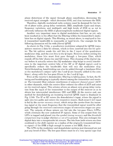
As shown in Fig. 2.34a, a quadrature modulator adopted for QPSK trans-
mitters receives a data bit stream, which is then inserted into the bit split-
ter. The bit splitter sends the odd bits to the I input of the quadrature
modulator chip, and the even bits to the Q input. However, before exiting the
modulator, these bits must first pass through a low-pass filter, which
rounds off the bits’ sharp rise and fall times. This shaping of the digital sig-
nal before it actually enters the I/Q modulator chip helps to avoid interfer-
ence to the important central lobe of the RF or IF digital signal—and to
specifically reduce the bandwidth that will exit the modulator chip.
Notwithstanding, bandlimiting can also be added through a bandpass filter
at the modulator’s output (after the I and Q are linearly added in the com-
biner), along with the low-pass filters in the I and Q legs.
Even at the receiver’s demodulator, filtering is taking place. In fact, the fil-
tering and bandshaping is typically shared among the transmitter and receiv-
er. The transmit filter reduces interference of adjacent channel power (ACP)
in other channels, while the receive filter reduces the effect of ACP and noise
on the received signal. This scheme allows an almost zero group delay varia-
tion from the input of the transmitter to the output of the receiver so as to
obtain low intersymbol interference (ISI) and BER. At the receive end, one
method for demodulating an incoming received QPSK input is displayed in
Fig. 2.34b. The IF or RF enters the demodulator’s input, where the signal is
split into two paths and enters the respective mixers. Each mixer’s LO input
is fed by the carrier recovery circuit, which strips the carrier from the incom-
ing signal at the exact frequency that the transmitted signal would be after
going through the receiver’s conversion stages (if conversion stages are pres-
ent). The outputs of these mixers are fed into the low-pass filters (LPFs),
which eliminate the now undesired IF signals. Some of this output from the
LPFs is tapped and placed into the symbol timing recovery and the threshold
comparison loop to judge whether a 1 or a 0 is present. This also reshapes the
digital data into a recognizable bit stream. The bits from both mixers are then
combined in the shift register as a replica of the originally transmitted bina-
ry signal—if the SNR is high enough to assure a low BER, that is.
The LPFs in the modulator and demodulator sections just discussed are not
just any breed of filter. The low-pass filters must be of a very special type that
Downloaded from Digital Engineering Library @ McGraw-Hill (www.digitalengineeringlibrary.com)
Copyright © 2004 The McGraw-Hill Companies. All rights reserved.
Any use is subject to the Terms of Use as given at the website.