
Page 305 - DSP Integrated Circuits
P. 305
290 Chapter 7 DSP System Design
twiddle factor in the first stage. The two alternatives will lead to similar solutions.
The only difference is the index generation, as just indicated.
An interesting observation is that for both alternatives the additions in the
index computation can be implemented by setting appropriate bits in the binary
representation of the index. For example, the index computations
in the second alternative need not be implemented as additions [15]. In the first
stage, k\ is in the range 0 to 255, but N s/2 is 256. Thus, it is sufficient to set bit 7 to 1.
We just assumed that integer m was incremented by 1 starting from 0 and
ending at JV/4 — 1. However, this scheme is unnecessarily restrictive. It is sufficient
that m take on all values in this range, the order is not important. One alternative
we will investigate later is to let the order of m be that of a Gray counter.
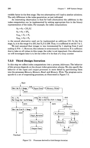
7.3.3 Third Design Iteration
In this step we collect index computations into a process, Addresses. The behavior
of this process depends on the chosen index generation scheme. We also specify the
behavior of the input and output processes in more detail by partitioning them
into the processes Memory, Memory_Read, and Memory_Write. The program corre-
sponds to a set of cooperating processes, as illustrated in Figure 7.5.
Figure 7.5 Processes derived in third design iteration