
Page 349 - DSP Integrated Circuits
P. 349
334 Chapter 7 DSP System Design
I I I I I I I I I I I I I I I
Rl \ A B
R2 j E ' I D |
"H mil! ! r^r^
"H : r^n!: i PA=I
0 1 2 3 4 5 6 7 8 9 10 11 12 13 14
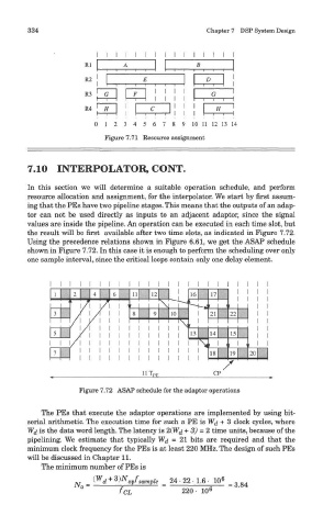
Figure 7.71 Resource assignment
7.10 INTERPOLATOR, CONT.
In this section we will determine a suitable operation schedule, and perform
resource allocation and assignment, for the interpolator. We start by first assum-
ing that the PEs have two pipeline stages. This means that the outputs of an adap-
tor can not be used directly as inputs to an adjacent adaptor, since the signal
values are inside the pipeline. An operation can be executed in each time slot, but
the result will be first available after two time slots, as indicated in Figure 7.72.
Using the precedence relations shown in Figure 6.61, we get the ASAP schedule
shown in Figure 7.72. In this case it is enough to perform the scheduling over only
one sample interval, since the critical loops contain only one delay element.
Figure 7.72 ASAP schedule for the adaptor operations
The PEs that execute the adaptor operations are implemented by using bit-
serial arithmetic. The execution time for such a PE is Wj + 3 clock cycles, where
Wd is the data word length. The latency is 2(W^ + 3) = 2 time units, because of the
pipelining. We estimate that typically W^ = 21 bits are required and that the
minimum clock frequency for the PEs is at least 220 MHz. The design of such PEs
will be discussed in Chapter 11.
The minimum number of PEs is