
Page 351 - DSP Integrated Circuits
P. 351
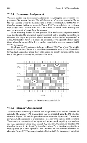
336                                             Chapter 7 DSP System Design


        7.10.1 Processor Assignment
        The next design step is processor assignment—i.e., mapping the processes onto
        processors. We assume that the PEs will share a set of common memories. Hence,
        the PEs can only access the memories one at a time. The executions of the PEs are
        therefore skewed in time, as shown in Figure 7.76. The sample interval is divided
        into 24 time slots. In each time slot a PE writes its result to the memory and
        receives a new set of inputs from the memory.
           There are many feasible PE assignments. This freedom in assignment may be
        used to minimize the amount of memory required and to simplify the control. In
        this case, the clique assignment scheme becomes too involved to be presented in
        detail. We therefore revert to a simple ad-hoc scheme. Two adjacent adaptor opera-
        tions, where the output of the first is used as input to the next, are assigned to PEi
        and PEa  +i) mod(4)-
           We choose the PE assignment shown in Figure 7.76. Two of the PEs are idle
        one-sixth of the time. Hence, it is possible to increase the order of the allpass filter
        to 9 and get a smoother group delay with almost no penalty in terms of the num-
        ber of PEs, power consumption, and execution time.


                           Figure 7.76 Skewed execution of the PEs


        7.10.2 Memory Assignment
        The constraints on memory allocation and assignment can be derived from the PE
        schedule. The memory-PE transactions can be extracted from the PE schedule
        shown in Figure 7.76 and the precedence form shown in Figure. 6.61. The arrows
        in Figure. 6.61 correspond to a transaction—i.e., one write and one read operation.
        There are four transactions (two inputs and outputs, each requiring one read and
        one write operation) taking place in each TPE time slot. The memory schedule will
        therefore be over 2 • 4 • 6 = 48T/if time slots, where TM is the time required for a
        memory read or a write operation. The lifetimes for the memory variables are
        shown in Figure 7.77. This chart is called a lifetime table for the memory variables.