
Page 139 - Electrical Properties of Materials
P. 139
Concluding remarks 121
E
Conduction
band
T=0
Energy
gap
Valence
band
(a)
F(E)
E
Conduction
T>>0 band
Energy
gap
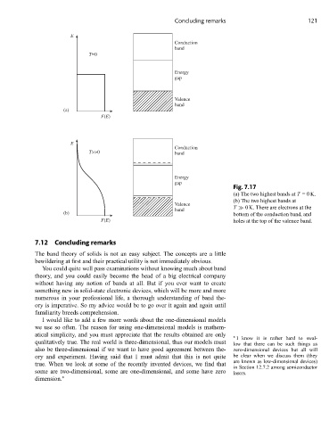
Fig. 7.17
(a) The two highest bands at T =0 K.
(b) The two highest bands at
Valence
band T 0 K. There are electrons at the
(b) bottom of the conduction band, and
F(E) holes at the top of the valence band.
7.12 Concluding remarks
The band theory of solids is not an easy subject. The concepts are a little
bewildering at first and their practical utility is not immediately obvious.
You could quite well pass examinations without knowing much about band
theory, and you could easily become the head of a big electrical company
without having any notion of bands at all. But if you ever want to create
something new in solid-state electronic devices, which will be more and more
numerous in your professional life, a thorough understanding of band the-
ory is imperative. So my advice would be to go over it again and again until
familiarity breeds comprehension.
I would like to add a few more words about the one-dimensional models
we use so often. The reason for using one-dimensional models is mathem-
atical simplicity, and you must appreciate that the results obtained are only
∗ I know it is rather hard to swal-
qualitatively true. The real world is three-dimensional, thus our models must low that there can be such things as
also be three-dimensional if we want to have good agreement between the- zero-dimensional devices but all will
ory and experiment. Having said that I must admit that this is not quite be clear when we discuss them (they
true. When we look at some of the recently invented devices, we find that are known as low-dimensional devices)
in Section 12.7.2 among semiconductor
some are two-dimensional, some are one-dimensional, and some have zero lasers.
dimension. ∗