
Page 156 - Electrical Properties of Materials
P. 156
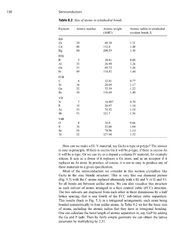
138                           Semiconductors

                                   Table 8.2 Size of atoms in tetrahedral bonds

                                   Element   Atomic number  Atomic weight  Atomic radius in tetrahedral
                                                            (AMU)          covalent bonds Å

                                   IIB
                                   Zn        30              68.38         1.31
                                   Cd        48             112.4          1.48
                                   Hg        80             200.59         1.48
                                   IIIB
                                   B          5              10.81         0.88
                                   Al        13              26.98         1.26
                                   Ga        31              69.72         1.26
                                   In        49             114.82         1.44
                                   IVB
                                   C          6              12.01         0.77
                                   Si        14              28.09         1.17
                                   Ge        32              72.59         1.22
                                   Sn        50             118.69         1.40
                                   VB
                                   N          7              14.007        0.70
                                   P         15              30.97         1.10
                                   As        33              74.92         1.18
                                   Sb        51             121.7          1.36
                                   VIB
                                   O          8              16.0          0.66
                                   S         16              32.06         1.04
                                   Se        34              78.96         1.14
                                   Te        52             127.60         1.32


                                     How can we make a III–V material, say GaAs n-type or p-type? The answer
                                   is easy in principle. If there is excess Ga it will be p-type, if there is excess As
                                   it will be n-type. Or we can try as a dopant a column IV material, for example
                                   silicon. It acts as a donor if it replaces a Ga atom, and as an acceptor if it
                                   replaces an As atom. In practice, of course, it is not so easy to produce any of
                                   these materials to a given specification.
                                     Most of the semiconductors we consider in this section crystallize like
                                   GaAs in the zinc blende structure. This is very like our diamond picture
                                   (Fig. 5.3) with the C atoms replaced alternately with a III and V or II and VI.
                                   So all bonds are between unlike atoms. We can also visualize this structure
                                   as each sub-set of atoms arranged in a face centred cubic (FCC) structure.
                                   The two sub-sets are displaced from each other in three dimensions by a half
                                   lattice spacing, that is one fourth of the FCC sub-lattice cubic separation.
                                   This results (back to Fig. 5.3) in a tetragonal arrangement, each atom being
                                   bonded symmetrically to four unlike atoms. In Table 8.2 we list the basic size
                                   of atoms, including the atomic radius that they have in tetragonal bonding.
                                   One can calculate the bond length of atomic separation in, say, GaP by adding
                                   the Ga and P radii. Then by fairly simple geometry we can obtain the lattice
                                   parameter by multiplying by 2.31.