
Page 159 - Electrical Properties of Materials
P. 159
Real semiconductors 141
The extra carriers are available for conduction as long as the semiconductor
is illuminated. What happens when the light is switched off? The number of
carriers must fall gradually to the equilibrium value. The time in which the ex-
tra density is reduced by a factor e = 2.718 is called the lifetime of the carrier
and is generally denoted by τ (and is thus quite often confused with the colli-
sion time). It is an important parameter in the design of many semiconductor
devices.
Assume now that only part of the semiconductor is illuminated; we shall
then have a region of high concentration in connection with regions of lower
concentration. This is clearly an unstable situation, and by analogy with gases,
we may expect the carriers to move away from places of high concentration
towards places of lower concentration. The analogy is incidentally correct; this
motion of the carriers has been observed, and can be described mathematically
by the usual diffusion equation D is the diffusion coefficient.
This equation is quite plausible
J = eD∇N. (8.56) physically; it means that if there
is a density gradient, a current
Equation (8.56) is equally valid for holes and electrons, though in a practical must flow.
case, the signs should be chosen with care.
8.8 Real semiconductors
All our relationships obtained so far have been based on some idealized model.
Perhaps the greatest distortion of reality came from our assumption of a simple
cubical lattice for the calculation of the band structure. As we know, silicon and
germanium crystallize in the diamond structure, and that makes a significant
difference.
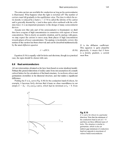
Plotting the E vs k x curve (Fig. 8.10) for the conduction band of silicon, for
example, it becomes fairly obvious that it bears no close resemblance to our
simple E = E 0 –2A x cos k x a curve, which had its minimum at k x =0. Even
E
E
g
Fig. 8.10
E–k curve for silicon in a particular
direction. Note that the minimum of
k the conduction band is not at k =0
x
0 and there are three different types of
holes. The situation is similar in
h
l germanium, which is also an
indirect-gap (minimum of conduction
band not opposite to maximum of
s
valence band) semiconductor.