Page 158 - Electrical Properties of Materials
P. 158

140                           Semiconductors

                                   Table 8.3 Semiconductor properties I. Energy gap and structure

                                   Semiconductor  Energy    Melting     Ionic %    Lattice spacing Å
                                                  gap eV    point K     of bond

                                   Group IV
                                   C              5.4        382         0         3.56
                                   Si             1.11      1680         0         5.43
                                   Ge             0.67      1210         0         5.66
                                   SiC            2.9                   18         3.08, 5.05
                                   Group III–V
                                   Al N           6.02      3070                   3.11, 4.98
                                   Al P           3.34      1770                   5.45
                                   Al As          2.2       1870                   5.66
                                   Al Sb          1.6       1330                   6.15
                                   Ga N           3.34      2770                   3.19, 5.18
                                   Ga P           2.24      1730                   5.45
                                   Ga As          1.42      1520        31         5.65
                                   Ga Sb          0.67       980        26         6.10
                                   In N           2.0       2475                   3.54, 5.70
                                   In P           1.27      1330        42         5.80
                                   In As          0.36      1215        36         6.06
                                   In Sb          0.17       798        32         6.48
                                   Group II–VI
                                   Zn O           3.20      2248        62         4.63
                                   Zn S           3.54      1925        62         5.41
                                   Zn Se          2.58      1790        63         5.67
                                   Zn Te          2.26      1658        61         6.10
                                   Cd O           2.5       2020        79
                                   Cd S           2.42      1750        69         5.58
                                   Cd Se          1.74      1512        70         6.05
                                   Cd Te          1.44      1368        67         6.48


                                   of molecular beam epitaxy (see Section 8.11.5) which makes it possible to
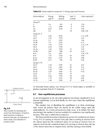
              Conduction band      produce junctions from II–VI materials.

      (i)   (ii)                   8.7  Non-equilibrium processes

                    (iii)          In our investigations so far, the semiconductor was always considered to be in
                                   thermal equilibrium. Let us look briefly at a few cases where the equilibrium
                                   is disturbed.
              Valence band
                                     The simplest way of disturbing the equilibrium is to shine electromag-
                                   netic waves (in practice these are mostly in the visible range) upon the
     Fig. 8.9
     Three models for obtaining free  semiconductor. As a result photoemission may occur, as in metals, but more
     carriers by illumination: (i) band-to-  interestingly, the number of carriers available for conduction may significantly
     band transitions yielding an  increase. This case is called photoconduction.
     electron–hole pair, (ii) ionization of  The three possible processes of producing carriers for conduction are shown
     donor atoms, (iii) ionization of  in Fig. 8.9; (i) creating an electron–hole pair, that is exciting an electron from
     acceptor atoms.               the valence band into the conduction band; (ii) exciting an electron from an
                                   impurity level into the conduction band; (iii) exciting an electron from the top
                                   of the valence band into an impurity level, and thus leaving a hole behind.
   153   154   155   156   157   158   159   160   161   162   163