
Page 160 - Electrical Properties of Materials
P. 160
142 Semiconductors
worse, the E vs k y curve would be very different from the one plotted. The
surfaces of constant energy in k-space are not spheres.
The situation is not much better in the valence band, where the constant en-
ergy surfaces are nearly spheres but—I regret to say—there are three different
types of holes present. This is shown in Fig. 8.10, where the letters h, l, and s
stand for heavy, light, and split-off bands respectively. What does it mean to
have three different types of holes? Well, just think of them as holes painted
red, blue, and green. They coexist peacefully, though occasionally, owing to
collisions, a hole may change its complexion.
Does this mean that all we have said so far is wrong? Definitely not. Does
it mean that considerable modifications are needed? No, for most purposes not
even that. We can get away with our simple model because, in general, only
average values are needed. It is nice to know that there are three different types
of holes in the valence band of silicon but for device operation only the average
effective mass and some sort of average collision time are needed.
The picture is not as black as it seems. In spite of the anisotropy in the E(k)
curves the grand total is isotropic. I mean that by performing all the relevant
averaging processes in silicon (still for a single-crystal material), the final res-
ult is an isotropic effective mass and isotropic collision time. Measuring the
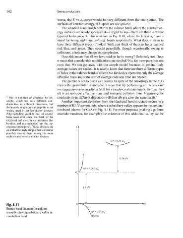
∗ This is not true of graphite, for ex- conductivity in different directions will thus always give the same result. ∗
ample, which has very different con- Another important deviation from the idealized band structure occurs in a
ductivities in different directions, but number of III–V compounds, where a subsidiary valley appears in the conduc-
fortunately single-crystal graphite is not
widely used in semiconductor devices. tion band (shown for GaAs in Fig. 8.11). For most purposes (making a gallium
Polycrystalline graphite has, of course, arsenide transistor, for example) the existence of this additional valley can be
been used ever since the birth of the
electrical and electronics industries (for
brushes and microphones) but the op-
erational principles of these devices are E
so embarrassingly simple that we cannot
possibly discuss them among the more
sophisticated semiconductor devices.
m*=0.35 m 0
0.36 eV
m*=0.067 m 0
E
g
1.4 eV
Fig. 8.11 0 k
Energy band diagram for gallium
arsenide showing subsidiary valley in m*=0.67 m 0
conduction band. (holes)