
Page 165 - Electrical Properties of Materials
P. 165
Measurement of semiconductor properties 147
Microwave
oscillator Circulator Receiver
1 3
Waveguide
2
Liquid helium
Dewar
flask
Sample
N S
Reflecting
plate
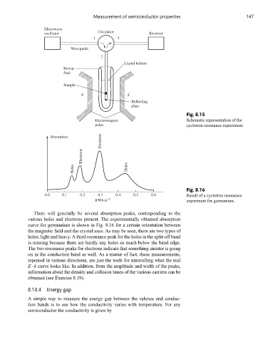
Fig. 8.15
Electromagnet Schematic representation of the
poles cyclotron resonance experiment.
Electrons
Absorption
Electrons
Holes Holes
Fig. 8.16
0.0 0.1 0.2 0.3 0.4 0.5 0.6 Result of a cyclotron resonance
BWbm –2 experiment for germanium.
There will generally be several absorption peaks, corresponding to the
various holes and electrons present. The experimentally obtained absorption
curve for germanium is shown in Fig. 8.16 for a certain orientation between
the magnetic field and the crystal axes. As may be seen, there are two types of
holes, light and heavy. A third resonance peak for the holes in the split-off band
is missing because there are hardly any holes so much below the band edge.
The two resonance peaks for electrons indicate that something sinister is going
on in the conduction band as well. As a matter of fact, these measurements,
repeated in various directions, are just the tools for unravelling what the real
E–k curve looks like. In addition, from the amplitude and width of the peaks,
information about the density and collision times of the various carriers can be
obtained (see Exercise 8.19).
8.10.4 Energy gap
A simple way to measure the energy gap between the valence and conduc-
tion bands is to see how the conductivity varies with temperature. For any
semiconductor the conductivity is given by