
Page 167 - Electrical Properties of Materials
P. 167
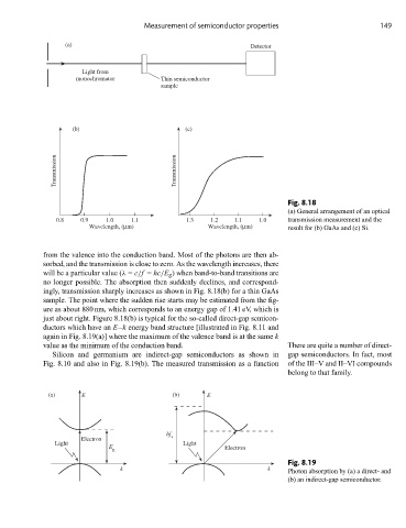
Measurement of semiconductor properties                       149

                  (a)                                              Detector


                       Light from
                     monochromator         Thin semiconductor
                                           sample


                      ) b (                        ) c (


                Transmission                   Transmission


                                                                             Fig. 8.18
                                                                             (a) General arrangement of an optical
                0.8   0.9    1.0    1.1           1.3    1.2   1.1   1.0     transmission measurement and the
                         Wavelength, (μm)               Wavelength, (μm)     result for (b) GaAs and (c) Si.


            from the valence into the conduction band. Most of the photons are then ab-
            sorbed, and the transmission is close to zero. As the wavelength increases, there
            will be a particular value (λ = c/f = hc/E g ) when band-to-band transitions are
            no longer possible. The absorption then suddenly declines, and correspond-
            ingly, transmission sharply increases as shown in Fig. 8.18(b) for a thin GaAs
            sample. The point where the sudden rise starts may be estimated from the fig-
            ure as about 880 nm, which corresponds to an energy gap of 1.41 eV, which is
            just about right. Figure 8.18(b) is typical for the so-called direct-gap semicon-
            ductors which have an E–k energy band structure [illustrated in Fig. 8.11 and
            again in Fig. 8.19(a)] where the maximum of the valence band is at the same k
            value as the minimum of the conduction band.                     There are quite a number of direct-
               Silicon and germanium are indirect-gap semiconductors as shown in  gap semiconductors. In fact, most
            Fig. 8.10 and also in Fig. 8.19(b). The measured transmission as a function  of the III–V and II–VI compounds
                                                                             belong to that family.


               ) a (   E                        ) b (   E


                                             hf
                      Electron                v
               Light                             Light
                              E                             Electron
                               g
                                                                             Fig. 8.19
                                 k                                      k    Photon absorption by (a) a direct- and
                                                                             (b) an indirect-gap semiconductor.