
Page 172 - Electrical Properties of Materials
P. 172
154 Semiconductors
the crystal so that the molten zone passes along its length. This technique can
be used only for fairly small crystals because the weight has to be supported
by the surface tension of the molten zone.
8.11.3 Modern methods of silicon purification
Nowadays an entirely different approach is taken to silicon purification. Silica
(SiO 2 ) is first reduced to metallurgical grade silicon (98% purity) by reacting
◦
◦
it with carbon in an electric arc furnace at 1900 C–2000 C. The solid is then
converted into a liquid, for example, by reaction with hydrochloric acid (HCl),
to form trichlorosilane (SiHCl 3 ) in a fluid bed reactor. This liquid is cooled
and condensed, and then purified by fractional distillation, a relatively simple
process. Finally, solid silicon with 99.999% purity is created by chemical va-
pour deposition onto high purity silicon rods or substrates, using a gas source
obtained by bubbling hydrogen through the trichlorosilane.
8.11.4 Epitaxial growth
The process of growing and refining single crystals made possible the advent
of the transistor in the 1950s. The next stage has been the planar technique,
starting in about 1960, that has led to the development of integrated circuits,
to be discussed in the next chapter. I shall just describe here the epitaxial
growth method of material preparation, which is eminently compatible with
the manufacture of integrated circuits.
∗
∗ My friends who speak ancient Greek ‘Epitaxial’ is derived from a Greek word meaning ‘arranged upon’. There
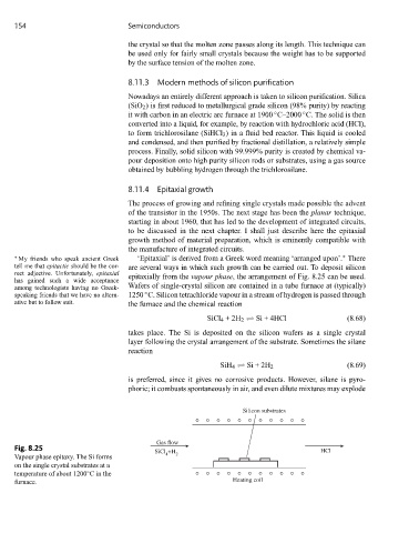
tell me that epitactic should be the cor- are several ways in which such growth can be carried out. To deposit silicon
rect adjective. Unfortunately, epitaxial epitaxially from the vapour phase, the arrangement of Fig. 8.25 can be used.
has gained such a wide acceptance
among technologists having no Greek- Wafers of single-crystal silicon are contained in a tube furnace at (typically)
◦
speaking friends that we have no altern- 1250 C. Silicon tetrachloride vapour in a stream of hydrogen is passed through
ative but to follow suit. the furnace and the chemical reaction
SiCl 4 +2H 2 Si + 4HCl (8.68)
takes place. The Si is deposited on the silicon wafers as a single crystal
layer following the crystal arrangement of the substrate. Sometimes the silane
reaction
SiH 4 Si + 2H 2 (8.69)
is preferred, since it gives no corrosive products. However, silane is pyro-
phoric; it combusts spontaneously in air, and even dilute mixtures may explode
Silicon substrates
Gas flow
Fig. 8.25
SiCl +H HCl
Vapour phase epitaxy. The Si forms 4 2
on the single crystal substrates at a
temperature of about 1200 Cinthe
◦
furnace. Heating coil