
Page 170 - Electrical Properties of Materials
P. 170
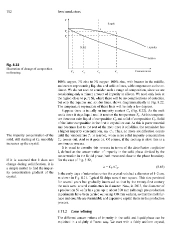
152                           Semiconductors

                                       T
                                                                Liquid
                                                           A
                                       T
                                        a
                                       T
                                        c

                                                Solid                                  Liquidus


                                                                                       Solidus
     Fig. 8.22
     Illustration of change of composition
                                          C      C        C         C           Concentration
     on freezing.                          b      d        a         c
                                   100% copper, 0% zinc to 0% copper, 100% zinc, with brasses in the middle,
                                   and curves representing liquidus and solidus lines, with temperature as the or-
                                   dinate. We do not need to consider such a range of composition, since we are
                                   considering only a minute amount of impurity in silicon. We need only look at
                                   the region close to pure Si, where there will be no complications of eutectics,
                                   but only the liquidus and solidus lines, shown diagrammatically in Fig. 8.22.
                                   The temperature separations of these lines will be only a few degrees.
                                     Suppose there is initially an impurity content C a (Fig. 8.22). As the melt
                                   cools down it stays liquid until it reaches the temperature T a . At this temperat-
                                   ure there can exist liquid of composition C a and solid of composition C b . Solid
                                   of the latter composition is the first to crystallize out. As this is purer material
                                   and becomes lost to the rest of the melt once it solidifies, the remainder has
                                   a higher impurity concentration, say C c . Thus, no more solidification occurs
     The impurity concentration of the  until the temperature T c is reached, when more solid impurity concentration
     solid, still starting at C b smoothly  C d comes out. And so it goes on. Of course, if the cooling is slow, this is a
     increases up the crystal.     continuous process.
                                     It is usual to describe this process in terms of the distribution coefficient
                                   k, defined as the concentration of impurity in the solid phase divided by the
                                   concentration in the liquid phase, both measured close to the phase boundary.
     If it is assumed that k does not  For the case of Fig. 8.22,
     change during solidification, it is
                                                             k = C b /C a .                 (8.65)
     a simple matter to find the impur-
     ity concentration gradient of the
                                   In the early days of microelectronics the crystal rods had a diameter of 1–2 cm,
     crystal.
                                   as shown in Fig. 8.21. Typical Si chips were 6 mm square. This size persisted
                                   for several years but gradually increased so that by the twenty-first century
                                   the rods were several centimetres in diameter. Now, in 2013, the diameter of
                                   a production Si wafer has gone up to about 300 mm (although pre-production
                                   experiments have been carried out using 450 mm wafers), so that the melt fur-
                                   nace and crucible are formidable and expensive capital items in the production
                                   process.

                                   8.11.2  Zone refining
                                   The different concentrations of impurity in the solid and liquid phase can be
                                   exploited in a slightly different way. We start with a fairly uniform crystal,