
Page 166 - Electrical Properties of Materials
P. 166
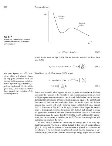
148                           Semiconductors


                                           log σ
                                             e
                                                          Intrinsic
                                                          region

                                                                             Extrinsic
                                                                             region


     Fig. 8.17
     Typical log conductivity–reciprocal
     temperature curve for an extrinsic
     semiconductor.                                                                  l/T


                                                         σ =(N e μ e + N h μ h )e,          (8.62)


                                   which is the same as eqn (8.45). For an intrinsic material, we have from
                                   eqn (8.46)

                                                                                –E g
                                                N e = N h = N i = constant × T 3/2  exp  .  (8.63)
                                                                              2kT

     We shall ignore the T 3/2  vari-  Combining eqn (8.62) with eqn (8.63) we get
     ation, which will almost always
     be negligible compared with the                                   3/2      E g
                                                σ = constant × e(μ e + μ h )T  exp –
     exponential temperature variation.                                        2kT
     Hence a plot of log σ versus 1/T                       E g
                    e
     will have a slope of –E g /2k, which         = σ 0 exp –   .                           (8.64)
                                                           2kT
     gives us E g . Also in eqn (8.64) we
     have ignored the variation of E g
                                   Let us now consider what happens with an impurity semiconductor. We have
     with temperature.
                                   discussed the variation of the Fermi level with temperature and concluded that
                                   at high temperatures semiconductors are intrinsic in behaviour, and at low tem-
                                   peratures they are pseudo-intrinsic with an energy gap equal to the gap between
                                   the impurity level and the band edge. Thus, we would expect two definite
                                   straight-line regions with greatly differing slopes on the plot of log σ against
                                                                                        e
                                   1/T, as illustrated in Fig. 8.17. In the region between these slopes the temper-
                                   ature is high enough to ionize the donors fully but not high enough to ionize
                                   an appreciable number of electrons from the host lattice. Hence, in this middle
                                   temperature range the carrier density will not be greatly influenced by temper-
                                   ature, and the variations in mobility and the T 3/2  factor that we neglected will
                                   determine the shape of the curve.
                                     An even simpler method of measuring the energy gap is to study op-
                                   tical transmission. The light is shone through a thin slice of semiconductor
                                   [Fig. 8.18(a)] and the amount of transmission is plotted as a function of
                                   wavelength. If the wavelength is sufficiently small (i.e. the frequency is suf-
                                   ficiently large), the incident photons have enough energy to promote electrons