
Page 163 - Electrical Properties of Materials
P. 163
Measurement of semiconductor properties 145
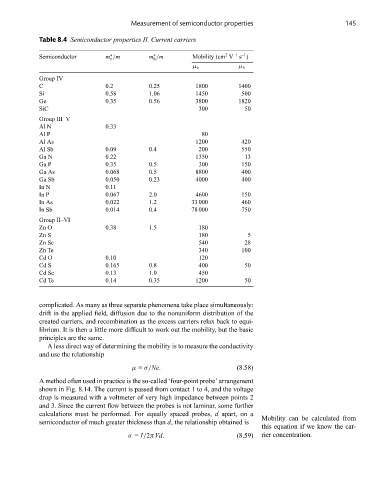
Table 8.4 Semiconductor properties II. Current carriers
–1 –1
2
∗
∗
Semiconductor m /m m /m Mobility (cm V s )
e
h
μ e μ h
Group IV
C 0.2 0.25 1800 1400
Si 0.58 1.06 1450 500
Ge 0.35 0.56 3800 1820
SiC 300 50
Group III–V
Al N 0.33
Al P 80
Al As 1200 420
Al Sb 0.09 0.4 200 550
Ga N 0.22 1350 13
Ga P 0.35 0.5 300 150
Ga As 0.068 0.5 8800 400
Ga Sb 0.050 0.23 4000 400
In N 0.11
In P 0.067 2.0 4600 150
In As 0.022 1.2 33 000 460
In Sb 0.014 0.4 78 000 750
Group II–VI
Zn O 0.38 1.5 180
Zn S 180 5
Zn Se 540 28
Zn Te 340 100
Cd O 0.10 120
Cd S 0.165 0.8 400 50
Cd Se 0.13 1.0 450
Cd Te 0.14 0.35 1200 50
complicated. As many as three separate phenomena take place simultaneously:
drift in the applied field, diffusion due to the nonuniform distribution of the
created carriers, and recombination as the excess carriers relax back to equi-
librium. It is then a little more difficult to work out the mobility, but the basic
principles are the same.
A less direct way of determining the mobility is to measure the conductivity
and use the relationship
μ = σ/Ne. (8.58)
A method often used in practice is the so-called ‘four-point probe’ arrangement
shown in Fig. 8.14. The current is passed from contact 1 to 4, and the voltage
drop is measured with a voltmeter of very high impedance between points 2
and 3. Since the current flow between the probes is not laminar, some further
calculations must be performed. For equally spaced probes, d apart, on a
Mobility can be calculated from
semiconductor of much greater thickness than d, the relationship obtained is
this equation if we know the car-
σ = I/2πVd. (8.59) rier concentration.