
Page 169 - Electrical Properties of Materials
P. 169
Preparation of pure and controlled-impurity single-crystal semiconductors 151
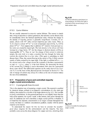
Light input
i
i
1
Fig. 8.20
Voltage
R (a) Photoconduction experiment in a
measured
Dark Current
+ – semiconductor. (b) When the light is
t Time switched off the current decays to its
(a) 1 (b) dark current value.
8.10.5 Carrier lifetime
We are usually interested in minority carrier lifetime. The reason is simply
that, owing to injection or optical generation, the minority carrier density may
be considerably above the thermal equilibrium value, whereas the change in
the density of majority carriers is generally insignificant. Consider, for ex-
ample, silicon with 10 22 fully ionized impurities per cubic metre. Then, as
16
N i for silicon is about 10 m –3 at room temperature [eqn (8.63)], N h will be
–3
10
about 10 m . Now suppose that in addition 10 15 electron–hole pairs per cu-
bic metre are created by input light. The hole density in the silicon will then
5
increase by a huge factor, 10 , but the change in electron density will be an
–5
imperceptible 10 %. Thus, to ‘see’ the change of hole current is relatively
simple; the only trick is to make a junction that lets through the holes but
restricts the electron flow to a low value. (This again is something we shall
discuss later.) Thus, the current flowing in the circuit of Fig. 8.20(a) consists
mainly of holes created by the input light. If the light is switched off at t = t 1 ,
the current (and so the voltage) across the resistance R declines exponentially
as exp{–(t – t 1 )/τ h }, where τ h is the hole lifetime. By measuring the decay
of the current [Fig. 8.20(b)] τ h can be determined. How does the exponential
decay come about? The differential equation can be easily derived (see Exer-
cise 8.17) on the basis of the physical picture developed in Section 8.5. The
rate of change of carriers may always be written as the rate of creation minus
the rate of recombination.
8.11 Preparation of pure and controlled-impurity
single-crystal semiconductors
8.11.1 Crystal growth from the melt
Molten
This is the simplest way of preparing a single crystal. The material is purified semiconductor
by chemical means, perhaps to an impurity concentration of a few parts per
million, then melted in a crucible of the shape shown in Fig. 8.21. The crucible Furnace walls
is slowly cooled down. As the pointed end tends to cool slightly faster than the
bulk of the material, the crystal ‘seeds’ at the bottom, then grows through the
melt. If conditions are well controlled, a single crystal growth is obtained. It
is found that the impurity concentration is no longer constant throughout the
crystal, but there is a definite concentration gradient, usually with the purest
Fig. 8.21
material at the bottom.
A form of crucible for melt-grown
To understand the reason for this we have to consider the metallur-
single crystals.
gical phase diagram for the semiconductor and the impurity. You have
probably come across the phase diagram for copper and zinc, stretching from