
Page 194 - Embedded Microprocessor Systems Real World Design
P. 194
Since the 1/0 decoding logic used partial address decode (see Chapter 2), I
actually sent the action codes to two different port addresses, specifically 3 and 4.
Address 3 got the action codes as just described and address 4 got the motor-speed
parameter. Both port addresses activated the 1/0 strobe that generated the capture
clock, but A0 was different for the two addresses. By connecting A0 as an input to
the logic analyzer, I was able to tell the data type of each captured byte.
This lengthy discussion about a specific 8031 system illustrates the kind of trace
information that can be captured using this type of debug method. Other methods
can be used to generate the trace information as well.
Write to ROM
In the followlng sections, ROM is used as a generic identifier for ROM,
PROM, or Flash memory.
In some systems, there are no spare 1/0 decodes. If the processor uses external
ROM, it often is possible to write debug information to the ROM space.
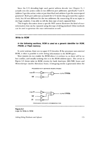
Most systems do not enable the ROM when it is written to, so there will be no
bus conflict, and usually nothing else is in the ROM address space. The circuit in
Figure 6.2 shows write to ROM circuits for both Intel-type (RD/WR) buses and
Motorola-type (strobe/direction) buses. A low-going strobe is generated when the
PROCESSOR WITH SEPARATE RDNR STROBES
ROM OUTPUT STROBE
-
WE
DS wF
ROM Cs
OUTPUT STROBE
PROCESSOR WITH DATA STROBElDlRECTlON
~ ~~~~
Figure 6.2
Logic for Write to ROM.
Adding Debug Hardware and Software 175