
Page 215 - Academic Press Encyclopedia of Physical Science and Technology 3rd Polymer
P. 215
P1: GOJ/GOI/LCC/HAR P2: GOJ Final Pages
Encyclopedia of Physical Science and Technology en012K-946 July 26, 2001 11:14
724 Polymers, Photoresponsive
Extreme ultraviolet (EUV) Refers to “soft” X-ray radi-
ation in the wavelength range of 13 to 25 nm.
Lithographic process (lithography) The process for
manufacturing semiconductor devices that involves
transferring a circuit pattern into a thin polymer film
and then transferring that pattern into the underlying
substrate.
Photoacid generator A molecule that generates acid
molecules upon irradiation. One class of such mate-
rials is the onium salts.
Post-exposure bake The baking step required for most
chemically amplified resists whereby the photo- or
radiation-generated acid catalytically reacts with pen-
dant groups on relevant resist components to effect a
change in solubility of the resist.
Resist (photoresist) A radiation- and/or photosensitive
polymer material that replicates the circuit pattern on a
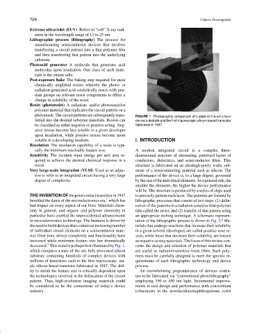
photomask. The circuit patterns are subsequently trans- FIGURE 1 Photographic comparison of a state-of-the-art silicon
ferred into the desired substrate materials. Resists can device substrate and the first macroscopic silicon-based transistor
be classified as either negative or positive acting. Neg- fabricated in 1947.
ative resists become less soluble in a given developer
upon irradiation, while positive resists become more
soluble in a developing medium. I. INTRODUCTION
Resolution The resolution capability of a resist is typi-
cally the minimum resolvable feature size. A modern integrated circuit is a complex three-
Sensitivity The incident input energy per unit area re- dimensional structure of alternating, patterned layers of
quired to achieve the desired chemical response in a conductors, dielectrics, and semiconductor films. This
resist. structure is fabricated on an ultrahigh-purity wafer sub-
Very large-scale integration (VLSI) Used as an adjec- strate of a semiconducting material such as silicon. The
tive to refer to an integrated circuit having a very large performance of the device is, to a large degree, governed
degree of complexity. bythesizeoftheindividualelements.Asageneralrule,the
smaller the elements, the higher the device performance
will be. The structure is produced by a series of steps used
THE INVENTION OF the point contact transistor in 1947 to precisely pattern each layer. The patterns are formed by
1
heralded the dawn of the microelectronics era, which has lithographic processes that consist of two steps: (1) delin-
had impact on every aspect of our lives. Materials chem- eation of the patterns in a radiation sensitive thin-polymer
istry in general, and organic and polymer chemistry in film called the resist, and (2) transfer of that pattern using
particular have enabled the unprecedented advancements an appropriate etching technique. A schematic represen-
2
in microelectronics technology. The business is driven by tation of the lithographic process is shown in Fig. 2. Ma-
theneedtobuild devicesthat containanincreasing number terials that undergo reactions that increase their solubility
of individual circuit elements on a semiconductor mate- in a given solvent (developer) are called positive-tone re-
rial. Over time, device complexity and functionality have sists, while those that decrease their solubility are known
increased while minimum feature size has dramatically as negative-acting materials. The focus of this review con-
2
decreased. This trend is perhaps best illustrated by Fig. 1, cerns the design and selection of polymer materials that
which compares a state-of-the-art, fully processed silicon are useful as radiation-sensitive resist films. Such poly-
substrate containing hundreds of complex devices with mers must be carefully designed to meet the specific re-
millions of transistors each to the first macrocscpic, sin- quirements of each lithographic technology and device
gle silicon-based transistor fabricated in 1947. The abil- process.
ity to shrink the feature size is critically dependent upon An overwhelming preponderance of devices contin-
the technologies involved in the delineation of the circuit ues to be fabricated via “conventional photolithography”
pattern. Thus, high-resolution imaging materials could employing 350 to 450 nm light. Incremental improve-
be considered to be the cornerstone of today’s device ments in tool design and performance with concomitant
industry. refinements in the novolac/diazonaphthoquinone resist