
Page 217 - Academic Press Encyclopedia of Physical Science and Technology 3rd Polymer
P. 217
P1: GOJ/GOI/LCC/HAR P2: GOJ Final Pages
Encyclopedia of Physical Science and Technology en012K-946 July 26, 2001 11:14
726 Polymers, Photoresponsive
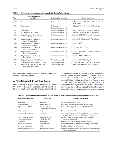
TABLE I Evolution of Lithographic and Semiconductor Device Technologies
Lithographic imaging
Year technology Resist imaging chemistry Device parameters
2
1967 Contact printing Cyclized rubber (–) 15–20 µm features; 256 DRAM; 0.2 cm device size;
1 Si substrate
2
1971 Near contact Cyclized rubber (–) 8–12 µm; 1K DRAM; 0.3 cm ;2 Si substrate
Novolac/diazoquinone (+)
2
1974 Near contact Novolac/diazoquinone (+) 6 µm; 4K DRAM; 0.4 cm ; 2.5 Si substrate
2
1977 1:1 projection; 360–420 nm Novolac/diazoquinone (+) 4 µm; 16K DRAM; 0.6 cm ;3 Si substrate
2
1980 Step and repeat; 5–10 × reduction Novolac/diazoquinone (+) <3 µm; 64K DRAM; 0.8 cm ;4 Si substrate
optics; 420–436 nm
2
1984 Step and repeat; 5 × reduction Novolac/diazoquinone (+) 1.5 µm; 256K DRAM; 1 cm ;6 Si substrate
optics; 436-nm (g-line)
1988 Step and repeat; 5 × reduction Novolac/diazoquinone (+) 0.9 µm; 1.8 cm 2
optics; 436-nm (g-line)
1990 Step and repeat; 5 × reduction Novolac/diazoquinone (+) 0.7 µm; 4M DRAM; 1.3 cm 2
optics; 365-nm (i-line)
2
1993 Step and repeat 5 × reduction Novolac/diazoquinone (+) 0.5 µm; 16M DRAM; 1.6 cm ;8 Si substrate
optics; 365-nm (i-line) introduced
1995 Step and repeat; 4–5 × (i-line); Novolac/diazoquinone (+) 0.35 µm; 64MB DRAM; 2 cm 2
deep-UV (248 nm)
1998 Step and repeat; deep-UV (248 nm) Chemically amplified 0.25 µm; 256M DRAM; 3 cm 2
2
2001 Step and repeat; deep-UV (248, 193 nm) Chemically amplified 0.18 µm; 1G DRAM; 5 cm ;8–12 Si wafers
2
2007 Deep-UV (193, 157 nm); EUV (13 nm); Chemically amplified <0.1 µm; 16G DRAM; 8 cm ;12 Si wafers
projection e-Beam; X-ray
available. The following sections outline the “traditional” ing this time consisted of cyclized poly(cis-1,4 isoprene)
9
materials chemistry options. and an aromatic azide crosslinking compound. The bis-
aryldiazide, 2,6-bis(4-azidobenzal)-4-methyl cyclohex-
anone, effectively initiates crosslinking of the matrix resin
A. Two-Component Crosslinking Resists
upon exposure to near-ultraviolet (UV) light (Fig. 3). The
During the early stages of the semiconductor indus- resolution of this highly sensitive, two-component resist
try (1957 to 1970), the minimum size of circuit fea- was limited due to solvent-induced swelling followed by
tures exceeded 5 µm, and the primary resist used dur- stress relaxation of the developed resist images. Enhanced
TABLE II Selected Resist Requirements as They Relate to Device Issues and Materials Molecular Characteristics
Lithographic parameter Device issue Molecular characteristic
Absorption Resolution No olefinic or aromatic moiety
Etching stability Process flexibility High levels of structural carbon, low oxygen content
Aqueous base solubility Process flexibility, Base solubilizing groups such as OH, COOH, NH, etc.
environmentally friendly
Substrate adhesion Yield Presence of polar moieties
Sensitivity (photospeed) Throughput Catalytic chain length for acidolysis, quantum yield for acid
generation, acid strength, protective group chemistry
Post-exposure delay and Resolution, process Catalytic chain length for acidolysis, protective group
substrate sensitivity flexibility, yield chemistry, acid strength
Outgassing Throughput Protective group and photoacid generator chemistry
Aspect ratio of images Resolution, yield Surface tension effects and mechanical strength of materials
Low metal ion content Yield Synthesis and scale-up methodology
Manufacturability and cost Manufacturing feasibility Synthesis and materials scale-up methodology and lithographic
process requirements