
Page 216 - Academic Press Encyclopedia of Physical Science and Technology 3rd Polymer
P. 216
P1: GOJ/GOI/LCC/HAR P2: GOJ Final Pages
Encyclopedia of Physical Science and Technology en012K-946 July 26, 2001 11:14
Polymers, Photoresponsive 725
II. POLYMER MATERIALS REQUIREMENTS
Resist chemistry must be carefully designed to meet the
specific requirements of a given lithographic technology.
Although these requirements vary according to the ra-
diation source, device process requirements, and expo-
sure tool design, the following are ubiquitous: sensitiv-
ity, contrast, resolution, etching resistance, purity, and
6
manufacturability. As noted in Table II, each of these
properties is affected by specific molecular characteristics
of the resin and can be tailored by careful manipulation
of polymer structure, molecular properties, and synthetic
methods. 7
The polymer resins must:
Exhibit solubility in solvents that allow the coating
of uniform, defect-free, thin films.
Be sufficiently thermally stable to withstand the
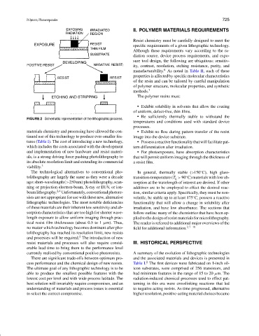
FIGURE 2 Schematic representation of the lithographic process.
temperatures and conditions used with standard device
processes.
materials chemistry and processing have allowed the con- Exhibit no flow during pattern transfer of the resist
tinued use of this technology to produce ever-smaller fea- image into the device substrate.
tures (Table I). The cost of introducing a new technology, Possess a reactive functionality that will facilitate pat-
which includes the costs associated with the development tern differentiation after irradiation.
and implementation of new hardware and resist materi- For photoexposure, have absorption characteristics
als, is a strong driving force pushing photolithography to that will permit uniform imaging through the thickness of
its absolute resolution limit and extending its commercial a resist film.
viability. 3
The technological alternatives to conventional pho- In general, thermally stable (>150 C), high glass-
◦
tolithography are largely the same as they were a decade transition-temperature (T g > 90 C) materials with low ab-
◦
ago: short-wavelength (>250 nm) photolithography, scan- sorption at the wavelength of interest are desired. If other
ning or projection electron-beam, X-ray or EUV, or ion- additives are to be employed to effect the desired reac-
beamlithography. 2,4 Unfortunately,conventionalphotore- tion, similar criteria apply. Specifically, they must be non-
sists are not appropriate for use with these new, alternative volatile, be stable up to at least 175 C, possess a reactive
◦
lithographic technologies. The most notable deficiencies functionality that will allow a change in solubility after
of these materials are their inherent low sensitivity and ab- irradiation, and have low absorbance. The sections that
sorption characteristics that are too high for shorter wave- follow outline many of the chemistries that have been ap-
length exposure to allow uniform imaging through prac- plied to the design of resist materials for microlithography.
tical resist film thicknesses (about 0.5 to 1 µm). Thus, The reader is referred to additional major overviews of the
no matter which technology becomes dominant after pho- field for additional information. 2,7−10
tolithography has reached its resolution limit, new resists
5
and processes will be required. The introduction of new
resist materials and processes will also require consid- III. HISTORICAL PERSPECTIVE
erable lead time to bring them to the performance level
currently realized by conventional positive photoresists. A summary of the evolution of lithographic technologies
There are significant trade-offs between optimum pro- and the associated materials and devices is presented in
2
cess performance and the chemical design of new resists. Table I. The first devices were fabricated on 1-inch sil-
The ultimate goal of any lithographic technology is to be icon substrates, were comprised of 256 transistors, and
able to produce the smallest possible features with the had minimum features in the range of 15 to 20 µm. The
lowest cost per level and with wide process latitude. The radiation-induced chemical processes used to effect pat-
best solution will invariably require compromises, and an terning in this era were crosslinking reactions that led
understanding of materials and process issues is essential to negative acting resists. As time progressed, alternative
to select the correct compromise. higher resolution, positive-acting material choices became