
Page 36 - Engineered Interfaces in Fiber Reinforced Composites
P. 36
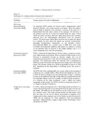
Chapter 2. Characterization of interfaces       19

               Table 2.4
               Techniques for studying s  ,urface structures and composition"
                                    ~~~
               Technique            Atomic process and type of information

                Microscopy
                Scanning electron   An  analytical  SEM  consists  of  electron  optics,  comprehensive  signal
                microscopy (SEM)    detection  facilities, and  a  high-vacuum environment.  When  the  primary
                                    electron  beam  is targctcd  at the  specimen, a  portion  of  the  electrons is
                                    backscattered  from  the  upper  surface of  the  specimen. The electrons in
                                    the  specimen can  also  be  excited  and  emitted  from  the  upper  surface
                                    which  are  called  secondary electrons.  Both  backscatterd  and  secondary
                                    electrons  carry  the  morphological  information  from  the  specimen
                                    surface. The microscope collects these electrons and transmits the signals
                                    to  a  cathode  ray  tube  where  the  signals  are  scanned  synchronously.
                                    providing  morphological  information  on  the  specimen  surface.
                                    Environmental  SEMs  are  a  special  type  of  SEM  that  work  under
                                    controlled  environmental  conditions and  require  no conductive  coating
                                    on  the  specimen with  the  pressure  in  the  sample chamber  only  1 or  2
                                    orders magnitude lower than the atmosphere.
               Transmission electron   TEM is composed of comprehensive electron optics, a projection system,
               microscopy (TEM)     and a high-vacuum environment. When a portion of high voltage primary
                                    electrons  is  transmitted  through  an  ultrathin  sample,  they  can  be
                                    unscattered and scattered to carry the microstructural  information of the
                                    specimen. The  microscopes collect  the  electrons  with  a  comprehensive
                                    detection system and project the microstructural images onto a fluorescent
                                    screen. The ultimate voltage for a TEM can generally be from  IO to  1000
                                    keV,  depending  on  the  requirement  of  resolving  power  and  specimcn
                                    thickness.
                Scanning tunneling   The STM, like other scanning probe microscopes, relies on the scanning of
                microscopy (STM)    a sharp tip over a sample surface. When the tip and sample are very close
                                    so that the electron clouds of tip and sample atoms overlap, a tunneling
                                    current can be established through voltage differences applied between the
                                    two electrodes. When a raster scan is made, the relative height coordinate z
                                    as  a  function  of  the  raster  coordinate  x  and  y  reflects  the  surface
                                    topography  of the sample. The STM is limited to conducting materials as
                                    it is based on the flow of electrons.
                Atomic forcc microscopy   In AFM, a sharp tip integrated with a soft spring (cantilever) deflects as a
                (AFM)               result of the local interaction forces present between the apex of the tip and
                                    the sample. The deflection of this cantilever can be monitored  at its rear
                                    by  a  distance sensor. The forces existing between tip  and sample, when
                                    they  are  close,  can  be  van  der  Waals,  electrostatic  or  magnetic  force.
                                    Atomic-scale friction, elasticity and surface forces can also be measured.
                                    AFM  can  be  employed  for  both  conductive  and  non-conductive
                                    specimens, without  having to apply  a  high  vacuum,  presenting a  major
                                    advantage over STM.