
Page 159 - Engineering Digital Design
P. 159
130 CHAPTER 3 / BACKGROUND FOR DIGITAL DESIGN
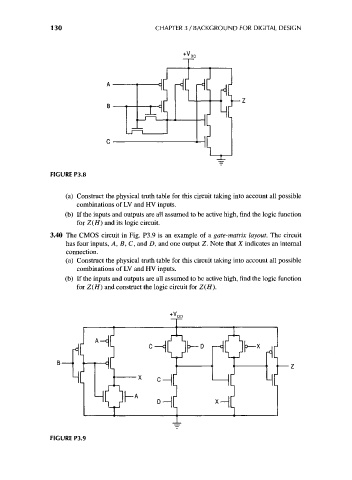
FIGURE P3.8
(a) Construct the physical truth table for this circuit taking into account all possible
combinations of LV and HV inputs.
(b) If the inputs and outputs are all assumed to be active high, find the logic function
for Z(H) and its logic circuit.
3.40 The CMOS circuit in Fig. P3.9 is an example of a gate-matrix layout. The circuit
has four inputs, A, B, C, and D, and one output Z. Note that X indicates an internal
connection.
(a) Construct the physical truth table for this circuit taking into account all possible
combinations of LV and HV inputs.
(b) If the inputs and outputs are all assumed to be active high, find the logic function
for Z(H) and construct the logic circuit for Z(H).
FIGURE P3.9