
Page 158 - Engineering Digital Design
P. 158
PROBLEMS 129
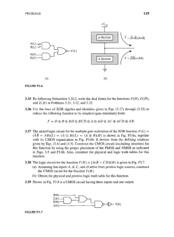
A(H)
B(H)
(a) (b)
FIGURE P3.6
3.35 By following Subsection 3.10.2, write the dual forms for the functions Y(H), G(H),
and Z(H) in Problems 3.21, 3.22, and 3.32.
3.36 Use the laws of XOR algebra and identities given in Eqs. (3.17) through (3.33) to
reduce the following function to its simplest (gate-minimum) form:
F = D 0 fl 0 #Z) 8 BCD 0 A 0 AD 0 AC 0 ACD 0 AB.
3.37 The mixed logic circuit for the multiple gate realization of the XOR function F(L) =
(AB + AB}(L) = (A O #)(£) = (A 0 #)(//) is shown in Fig. P3.6a, together
with its CMOS organization in Fig. P3.6b. It derives from the defining relations
given by Eqs. (3.4) and (3.5). Construct the CMOS circuit (excluding inverters) for
this function by using the proper placement of the PMOS and NMOS as indicated
in Figs. 3.5 and P3.6b. Also, construct the physical and logic truth tables for this
function.
3.38 The logic circuit for the function Y(H) = [A(B + CD)](H) is given in Fig. P3.7.
(a) Assuming that inputs A, B, C, and D arrive from positive logic sources, construct
the CMOS circuit for the function Y(H).
(b) Obtain the physical and positive logic truth table for this function.
3.39 Shown in Fig. P3.8 is a CMOS circuit having three inputs and one output.
B(H)-
C(H) —
D(H) —
A(H)-
FIGURE P3.7