
Page 154 - Engineering Digital Design
P. 154
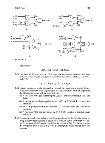
PROBLEMS                                                            125


                A(H)                                                         W(L)
                             1
                                          y~* Z(H)                               ~~^    'Y(H)
                D(H)
                                                             (H)-^rr^        1" ^-^
                                                                   __n ^
                                                            .   -v x r^J  y j  v / LJ \
                                                      C(H)-D
                            (a)


            C(H)


                               (c)                           0(L)

                  FIGURE P3.3

                      logic sources.

                                          G(H) = [(X Y) ® Z +
                 3.23 Use three NAND gates and two EQV gates (nothing else) to implement the func-
                      tion F(H ) below exactly as written. Assume the inputs arrive as W(L), X(L), Y(H),
                      and Z(H}.

                                        F(H) = [(W 07)© (XZ) + WY](H)

                 3.24 Unused inputs must not be left dangling. Instead, they must be tied to other inputs,
                      or be connected to HV or LV depending on the logic operations involved. Implement
                      the following functions with the logic indicated.
                      (a) A four-input NOR gate performing the (AB)(H) operation with inputs A(L) and
                         B(H).
                      (b) A three-input NAND gate performing the X(H) — > X(L) logic level conversion
                         operation.
                      (c) An XOR gate performing the controlled X(L) —> X(H} logic level conversion
                         operation.
                      (d) A four-input AND gate performing the (A + fi)(L) operation with inputs A(H)
                         and
                 3.25 Construct the truth table and the mixed logic waveforms for the functions below by
                      using a binary input sequence in alphabetical order, all inputs active high. Use Ta-
                      ble 2.1 in Section 2.3 if needed, and follow the format of Fig. 3.32 in constructing
                      the waveforms. Do not take into account the propagation delays through gates and
                      inverters.